Check patentability & draft patents in minutes with Patsnap Eureka AI!

Semiconductor device with negative capacitance material in buried channel

a negative capacitance material and semiconductor technology, applied in semiconductor devices, capacitors, electrical devices, etc., can solve the problem that the threshold voltage can affect the read/write operation speed of buried-channel array transistors

Active Publication Date: 2021-03-02
NAN YA TECH
View PDF3 Cites 2 Cited by
  • Summary
  • Abstract
  • Description
  • Claims
  • Application Information

AI Technical Summary

Benefits of technology

The integration of a negative capacitance material layer increases the read / write operation speed by enabling faster charging and discharging, reducing leakage current, and improving overall DRAM performance.

Problems solved by technology

However, the read / write operation speed of the buried-channel array transistor can be affected by the threshold voltage.

Method used


Image

  • Semiconductor device with negative capacitance material in buried channel
  • Semiconductor device with negative capacitance material in buried channel
  • Semiconductor device with negative capacitance material in buried channel

Examples


Embodiment Construction

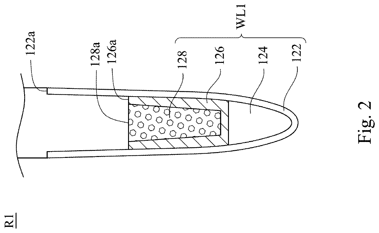
[0034]Reference will now be made in detail to the present embodiments of the invention, examples of which are illustrated in the accompanying drawings. Wherever possible, the same reference numbers are used in the drawings and the description to refer to the same or like parts.

[0035]The following disclosure provides many different embodiments, or examples, for implementing different features of the provided subject matter. Specific examples of components and arrangements are described below to simplify the present disclosure. These are, of course, merely examples and are not intended to be limiting. For example, the formation of a first feature over or on a second feature in the description that follows may include embodiments in which the first and second features are formed in direct contact, and may also include embodiments in which additional features may be formed between the first and second features, such that the first and second features may not be in direct contact. In add...


PUM

PropertyMeasurementUnit
thicknessaaaaaaaaaa
thicknessaaaaaaaaaa
depth d1aaaaaaaaaa

Abstract

A semiconductor device includes a substrate, at least one trench, an insulating layer, a lower metal layer, a negative capacitance material layer, and an upper metal layer. The trench has an inner surface in the substrate. The insulating layer is disposed on and lining the inner surface of the trench. The lower metal layer is disposed on the insulating layer and partially filling the trench. The negative capacitance material layer is disposed on and lining the insulating layer and the lower metal layer, in which a remained portion of the trench is defined by the negative capacitance material layer. The upper metal layer is disposed on the negative capacitance material layer and filling the remained portion of the trench.

Description

CROSS-REFERENCE TO RELATED APPLICATION[0001]This application claims priority to U.S. Provisional Application Ser. No. 62 / 775,916, filed Dec. 6, 2018, which is herein incorporated by reference.BACKGROUNDField of Invention[0002]The present invention relates to a semiconductor device. More particularly, the present invention relates to semiconductor device having a negative capacitance material layer in a buried channel.Description of Related Art[0003]A DRAM device may include a plurality of buried-channel array transistor (BCAT). The buried-channel array transistor has a longer effective channel length compared with a planar transistor as its gate electrode is buried under a semiconductor substrate, such that the DRAM device may be downsized and the integration density thereof can be increased.[0004]However, the read / write operation speed of the buried-channel array transistor can be affected by the threshold voltage. Specifically, when the threshold voltage of the buried-channel arra...

Claims


Application Information

Patent Timeline
Patent Type & Authority Patents(United States)
IPC IPC(8): H01L29/51H01L29/78H01L29/423
CPCH01L29/516H01L29/4236H01L29/517H01L29/7827H01L29/0688H01L29/78H01L28/40H10B12/312H10B12/0335H10B53/30
Inventor HUANG, CHING-CHIALU, TSENG-FULIAO, WEI-MING
Owner NAN YA TECH
Features
  • R&D
  • Intellectual Property
  • Life Sciences
  • Materials
  • Tech Scout
  • Unparalleled Data Quality
  • Higher Quality Content
  • 60% Fewer Hallucinations
Learn More