Pixel structure

a technology of pixel structure and pixel shape, which is applied in the direction of basic electric elements, semiconductor devices, electrical equipment, etc., can solve the problems of low manufacturing yield of micro led display devices, inability to drive normally, and small size of led elements, so as to reduce the degree of uneven brightness of light-emitting diodes caused by process variations , the effect of improving manufacturing yield

Active Publication Date: 2021-03-23
AU OPTRONICS CORP
View PDF17 Cites 0 Cited by
  • Summary
  • Abstract
  • Description
  • Claims
  • Application Information

AI Technical Summary

Benefits of technology

[0005]The present invention provides a pixel structure, so that a manufacturing yield can be improved and the degree of unevenness of the brightness of light-emitting diode elements caused by process variations can be reduced.

Problems solved by technology

However, today's display devices are generally provided with millions of pixels, and LED elements are small in size and difficult to precisely pick up and align.
Consequently, the LED elements cannot be accurately placed at a preset position due to alignment errors, leading to a problem that the LED elements cannot be driven normally.
In other words, currently, a manufacturing yield of the micro LED display device is low.
Moreover, unevenness of the brightness of the LED elements may be caused by process variations.

Method used


Image

  • Pixel structure
  • Pixel structure
  • Pixel structure

Examples


Embodiment Construction

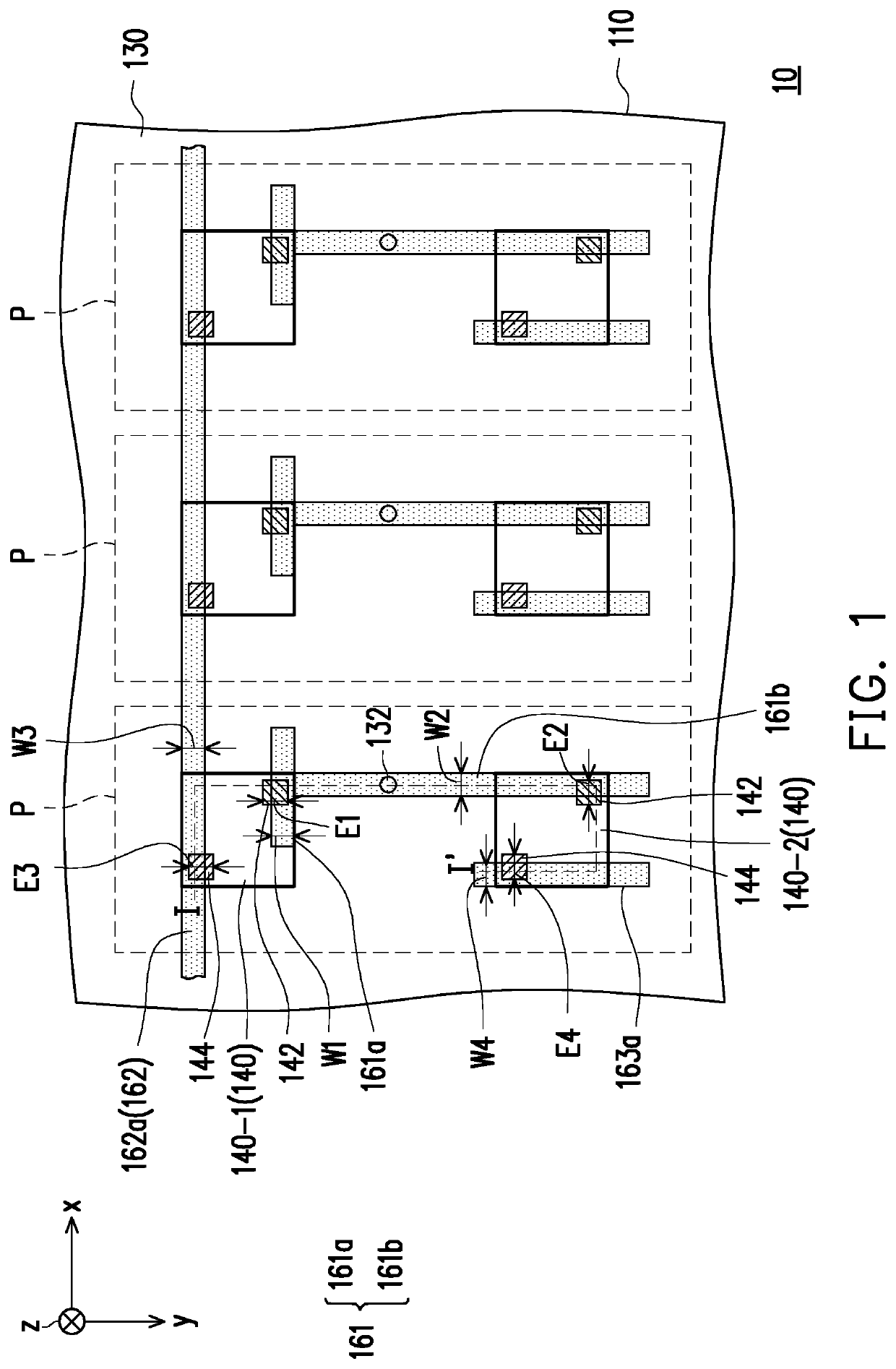
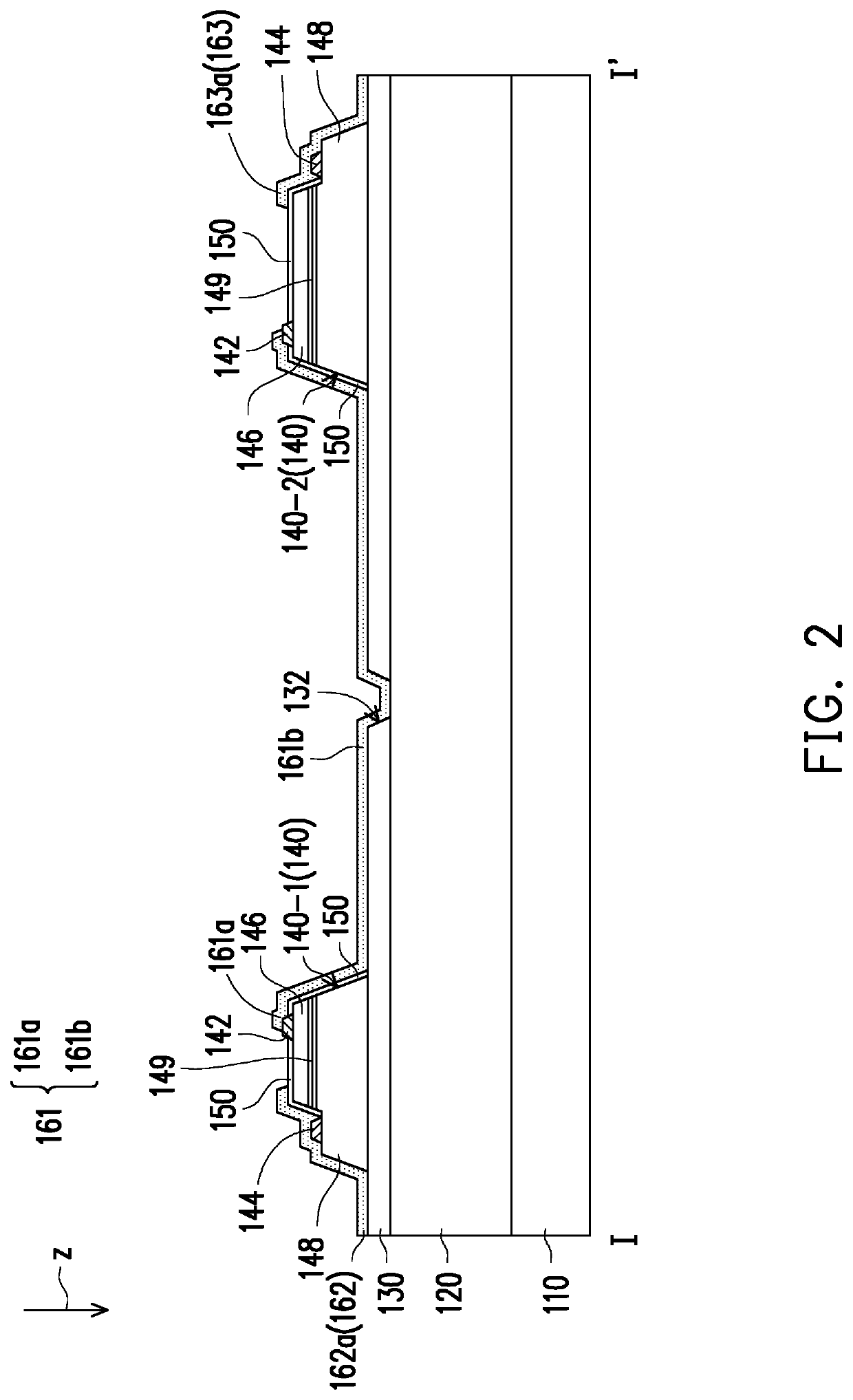
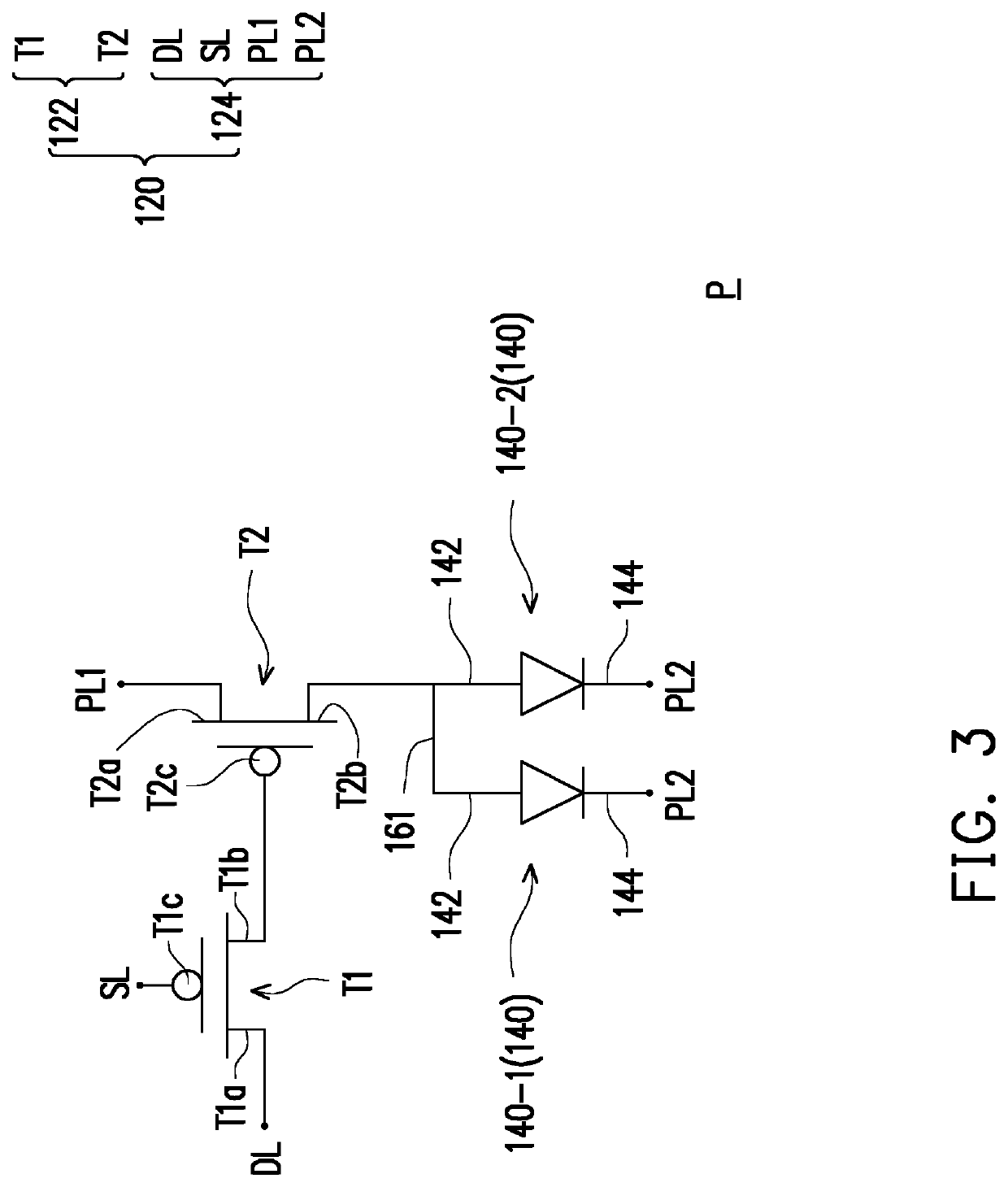
[0035]Reference will now be made in detail to the present exemplary embodiments of the present invention, examples of which are illustrated in the accompanying drawings. Wherever possible, the same element numbers are used in the drawings and the description to refer to the same or like parts.

[0036]It will be understood that, when an element such as a layer, a film, an area or a substrate is referred to as being “on” or “connected” to another element, the element may be directly on another element, or connected to another element, or there may be an intermediate element. In contrast, when an element is referred to as “directly on” or “directly connected to” another element, there is no intermediate element. As used herein, “connected” may refer to both physical and / or electrical connections. Furthermore, “electrically connected” or “coupling” may be the presence of other elements between two elements.

[0037]As used herein, “about,”“approximate,” or “substantially” includes the values...


PUM

PropertyMeasurementUnit
lengthaaaaaaaaaa
lengthaaaaaaaaaa
widthaaaaaaaaaa

Abstract

A pixel structure including a first light-emitting diode element, a second light-emitting diode element and a first interconnection pattern is provided. The first interconnection pattern is disposed on and electrically connected to a first electrode of the first light-emitting diode element and a first electrode of the second light-emitting diode element. The first interconnection pattern is configured to be electrically connected to a drive element. The first interconnection pattern includes a first main portion and a second main portion. The first main portion extending in a first direction is disposed on the first electrode of the first light-emitting diode element. The second main portion extending in a second direction and connected to the first main portion is disposed on the first electrode of the second light-emitting diode element. The first direction and the second direction are crossed.

Description

CROSS-REFERENCE TO RELATED APPLICATION[0001]This application claims the priority benefit of Taiwan application serial no. 107143901, filed on Dec. 6, 2018. The entirety of the above-mentioned patent application is hereby incorporated by reference herein and made a part of this specification.BACKGROUND OF THE INVENTION1. Field of the Invention[0002]The present invention relates to a pixel structure, and in particular, to a pixel structure including a plurality of light-emitting diode elements.2. Description of Related Art[0003]With the development of display technologies, thin display devices with a high resolution are popular in the mainstream market. In recent years, due to a breakthrough in manufacturing technologies of light-emitting diode (LED) elements, micro LED display devices or millimeter-grade LED display devices, or the like that can be manufactured by arranging LED elements in an array are developed. A liquid crystal layer and a color filter do not need to be provided in...

Claims


Application Information

Patent Timeline
Patent Type & Authority Patents(United States)
IPC IPC(8): H01L27/12H01L27/06H01L25/16
CPCH01L27/124H01L25/167H01L27/0617H01L33/62H01L2224/24
Inventor HUANG, PU-JUNGLIU, PIN-MIAOTSAI, CHENG-YEH
Owner AU OPTRONICS CORP
Why Eureka
Try Eureka