Memory interface circuit, memory storage device and signal generation method

a memory storage device and signal generation technology, applied in the field of memory interface technology, to achieve the effect of improving the efficiency of signal transmission

Active Publication Date: 2021-04-13
PHISON ELECTRONICS
View PDF7 Cites 0 Cited by
  • Summary
  • Abstract
  • Description
  • Claims
  • Application Information

AI Technical Summary

Benefits of technology

[0007]The invention provides a memory interface circuit, a memory storage device and a signal generation method, which can effectively improve a signal transmission efficiency.
[0014]Based on the above, in certain exemplary embodiments, the command signal and the address signal can be respectively provided to the volatile memory module based on the rising edge and the falling edge (or the falling edge and the rising edge) of the reference clock signal, and / or in certain exemplary embodiments, the command signal and the address signal provided to the volatile memory module can have the different transmission cycles. As a result, the signal transmission efficiency between the memory interface circuit and the volatile memory module can be effectively improved.

Problems solved by technology

However, because such a transmission mechanism will have a relatively strong interference between the signals, a signal receiver and / or a signal transmitter need to have a strong anti-noise capability in order to accurately transmit data.

Method used


Image

  • Memory interface circuit, memory storage device and signal generation method
  • Memory interface circuit, memory storage device and signal generation method
  • Memory interface circuit, memory storage device and signal generation method

Examples


Embodiment Construction

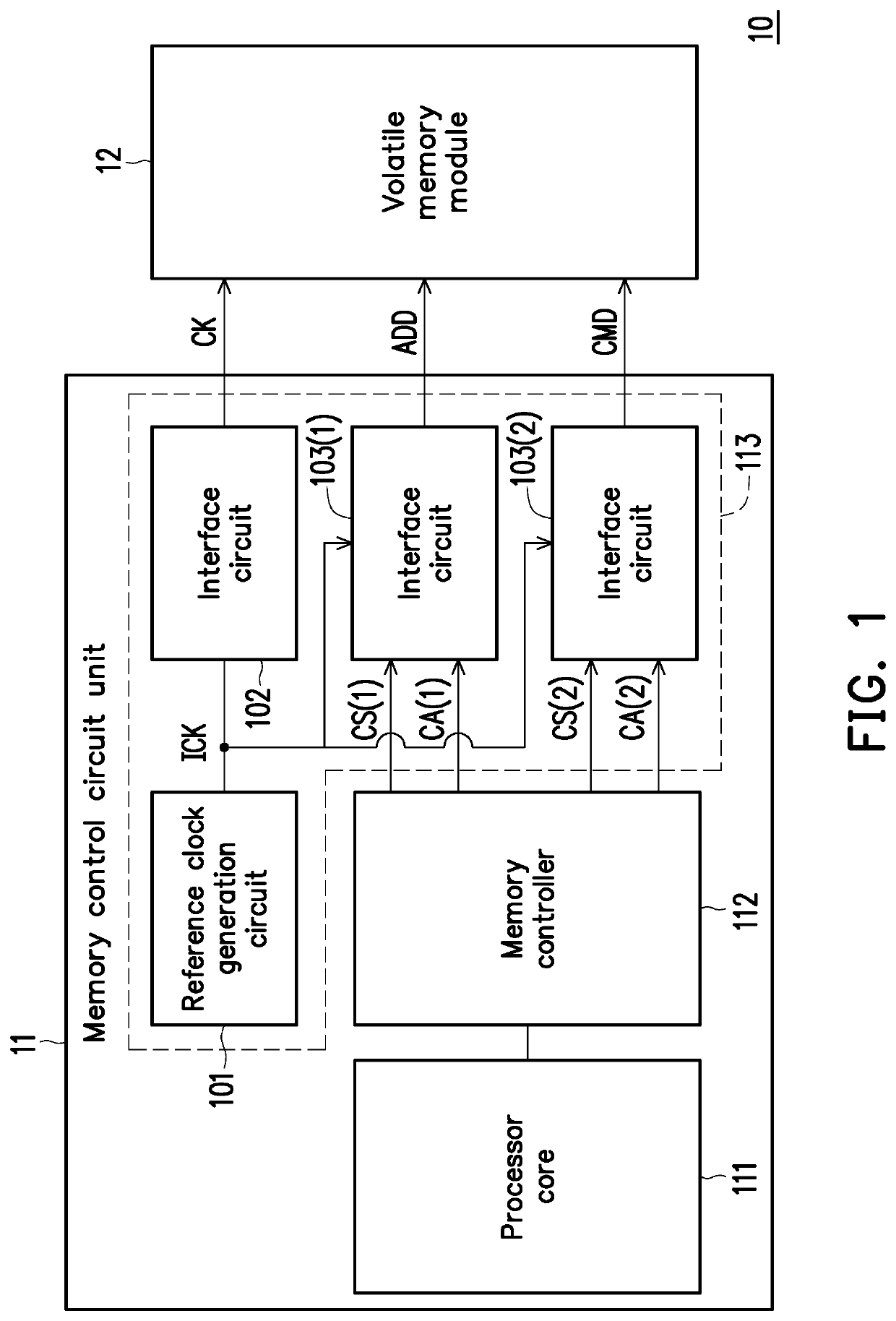
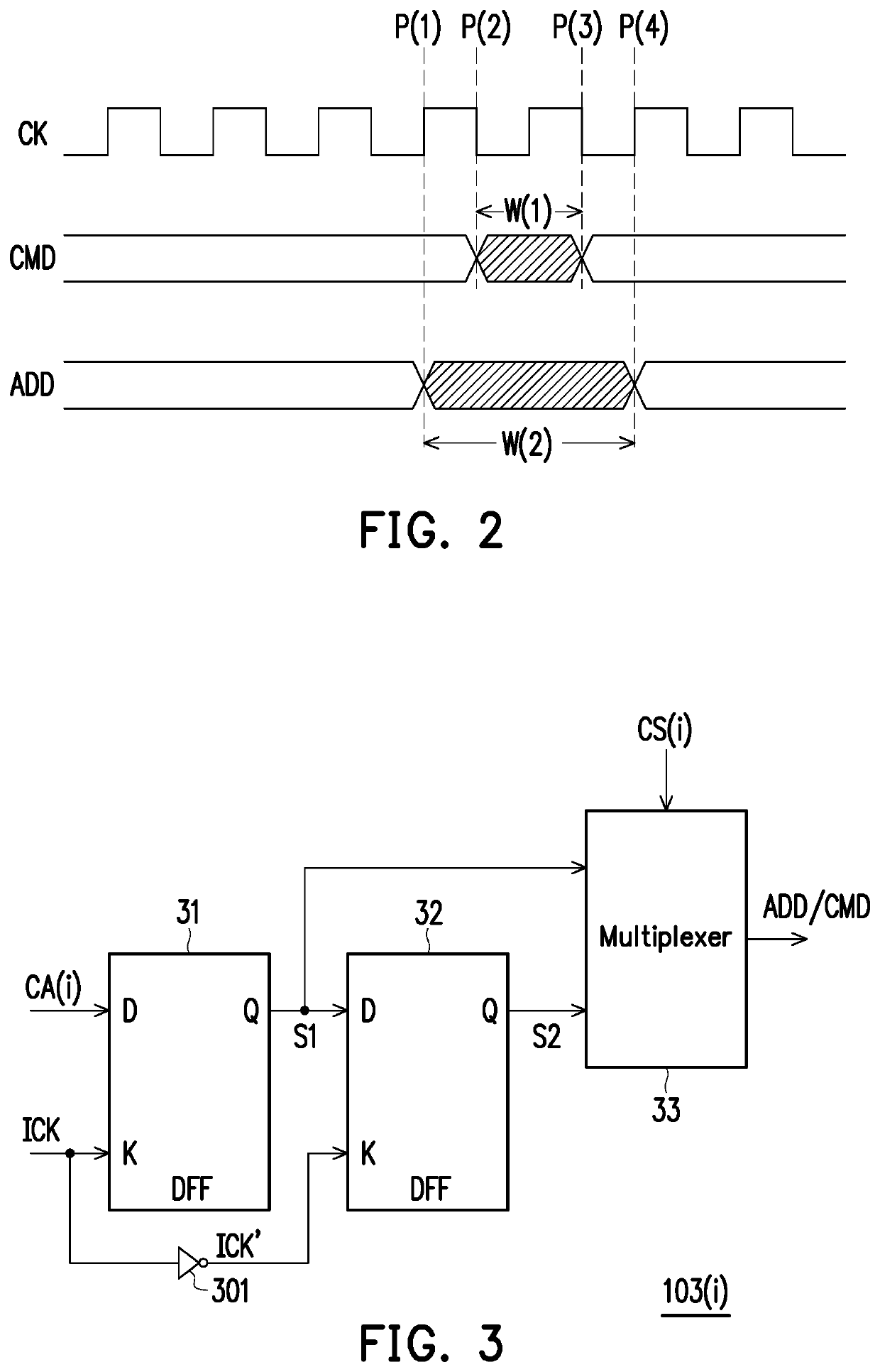
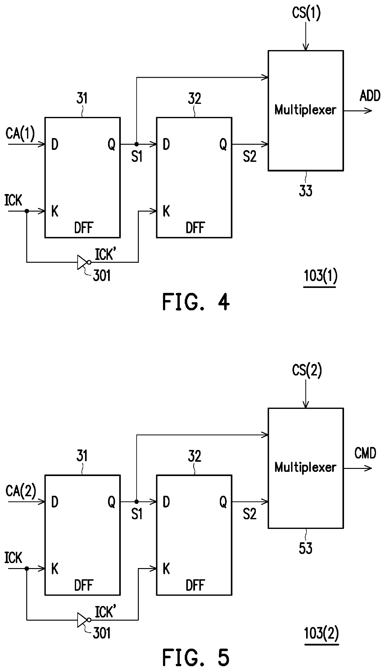
[0026]Reference will now be made in detail to the present preferred embodiments of the invention, examples of which are illustrated in the accompanying drawings. Wherever possible, the same reference numbers are used in the drawings and the description to refer to the same or like parts.

[0027]Embodiments of the present invention may comprise any one or more of the novel features described herein, including in the Detailed Description, and / or shown in the drawings. As used herein, “at least one”, “one or more”, and “and / or” are open-ended expressions that are both conjunctive and disjunctive in operation. For example, each of the expressions “at least one of A, B and C”, “at least one of A, B, or C”, “one or more of A, B, and C”, “one or more of A, B, or C” and “A, B, and / or C” means A alone, B alone, C alone, A and B together, A and C together, B and C together, or A, B and C together.

[0028]It is to be noted that the term “a” or “an” entity refers to one or more of that entity. As s...


PUM


Abstract

A memory interface circuit, a memory storage device and a signal generation method are provided. The memory interface circuit is configured to connect a volatile memory module and a memory controller. The memory interface circuit includes a clock generation circuit, a first interface circuit and a second interface circuit. The clock generation circuit is configured to provide a reference clock signal. The first interface circuit is configured to provide an address signal to the volatile memory module based on a first transition point of the reference clock signal. The second interface circuit is configured to provide a command signal to the volatile memory module based on a second transition point of the reference clock signal. The first transition point is one of a rising edge and a falling edge of the reference clock signal. The second transition point is the other one of the rising edge and the falling edge of the reference clock signal.

Description

CROSS-REFERENCE TO RELATED APPLICATION[0001]This application claims the priority benefit of Taiwan application serial no. 108126253, filed on Jul. 24, 2019. The entirety of the above-mentioned patent application is hereby incorporated by reference herein and made a part of this specification.BACKGROUNDTechnical Field[0002]The invention relates to a memory interface technology, and more particularly, relates to a memory interface circuit, a memory storage device and a signal generation method.Description of Related Art[0003]The markets of digital cameras, cellular phones, and MP3 players have expanded rapidly in recent years, resulting in escalated demand for storage media by consumers. The characteristics of data non-volatility, low power consumption, and compact size make a rewritable non-volatile memory module (e.g., flash memory) ideal to be built in the portable multi-media devices as cited above.[0004]Most memory storage devices are disposed with a volatile memory module (e.g.,...

Claims


Application Information

Patent Timeline
Patent Type & Authority Patents(United States)
IPC IPC(8): G11C7/22G11C11/40G11C11/4096G11C11/408G11C11/4093G11C11/4076
CPCG11C7/227G11C7/222G11C11/408G11C11/4076G11C11/4093G11C11/4096G06F13/1657G11C7/02G11C7/109G11C11/409
Inventor HUANG, MING-CHIEN
Owner PHISON ELECTRONICS
Why Eureka
Try Eureka