Eureka AIR delivers breakthrough ideas for toughest innovation challenges, trusted by R&D personnel around the world.

Polyimide film for semiconductor package reflow process, and manufacturing method therefor

a technology of polyimide film and semiconductor chips, which is applied in the direction of film/foil adhesives, transportation and packaging, synthetic resin layered products, etc., can solve the problems that conventional polyimide films are not easily attached to and detached from semiconductor chips after reflow, and achieve the effect of easy attachment and detached

Active Publication Date: 2021-05-25
IPI TECH
View PDF14 Cites 0 Cited by
  • Summary
  • Abstract
  • Description
  • Claims
  • Application Information

AI Technical Summary

Benefits of technology

[0013]In relation to a polyimide film for a semiconductor package reflow process and a manufacturing method therefor according to the present invention, an aromatic diamine containing any one of an ether group, a ketone group and a methyl group and an aromatic dianhydride containing any one of an ether group, a ketone group and a methyl group are synthesized in an organic solvent so as to produce a polyamic acid, and the polyamic acid is used for a thermoplastic polyimide layer. Accordingly, the thermoplastic polyimide layer may have glass transition temperature of 260° C. or lower.
[0014]That is, in relation to a polyimide film for a semiconductor package reflow process and a manufacturing method therefor according to the present invention, the thermoplastic polyimide layer having glass transition temperature of 260° C. or lower is applied to a polyimide film such that the releasing property of the polyimide film is ensured after reflow, thereby enabling the polyimide film to be easily attached to and detached from a semiconductor chip.
[0015]Additionally, in relation to a polyimide film for a semiconductor package reflow process and a manufacturing method therefor according to the present invention, a thermoplastic polyimide layer the surface of which is modified with a carboxyl group is applied to a polyimide film such that the adhesive force between the thermoplastic polyimide layer and an adhesive layer is significantly increased.

Problems solved by technology

However, such conventional polyimide films are not easily attached to and detached from semiconductor chips after reflow.As a related art document, Korean Patent Laid-Open Publication No. 10-2014-0084095 (published on Jul. 4, 2014) is disclosed.

Method used


Image

  • Polyimide film for semiconductor package reflow process, and manufacturing method therefor
  • Polyimide film for semiconductor package reflow process, and manufacturing method therefor
  • Polyimide film for semiconductor package reflow process, and manufacturing method therefor

Examples


Embodiment Construction

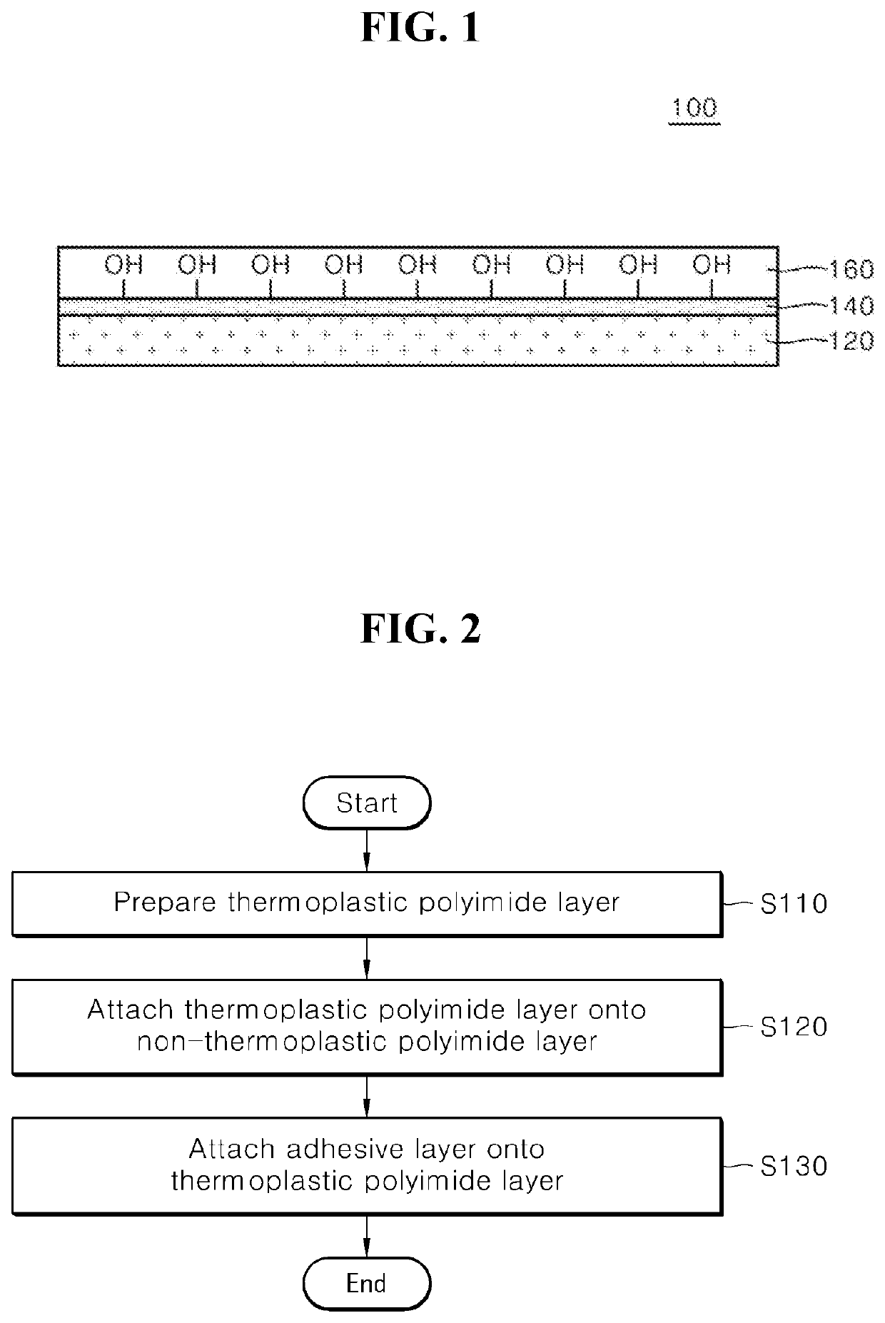
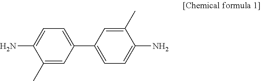
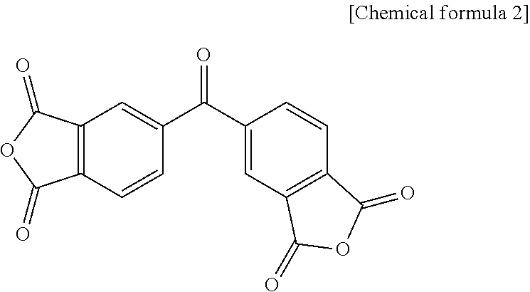
[0072]First, 36.6 g of 3,3′-dimethyl-[1,1′-biphenyl]-4,4′-diamine and 53.4 g of 3,3′,4,4′-benzophenonetetracarboxylic dianhydride were polymerized in 410 g of NMP so as to synthesize a polyamic acid, and 6 μm of the polyamic acid was applied onto a thermosetting polyimide film and then heated at 350° C. such that a thermoplastic polyimide layer was formed.

[0073]Next, an acrylic adhesive layer was attached onto the thermoplastic polyimide layer such that a polyimide film was manufactured.

[0074]2. Evaluating Physical Properties

[0075]Table 1 shows evaluated physical properties of a polyimide film manufactured according to embodiments 1 to 3 and comparison 1.

[0076]1) Glass Transition Temperature

[0077]Glass transition temperature of a thermoplastic polyimide layer was measured with Q400 of TA Instruments.

[0078]2) Adhesive Force

[0079]A polyimide film is cut to have a width of 100 mm and a length of 100 mm and press-heated at 260° C. and 500 kgf, and the adhesive force between a thermoplas...


PUM

PropertyMeasurementUnit
glass transition temperatureaaaaaaaaaa
temperaturesaaaaaaaaaa
glass transition temperatureaaaaaaaaaa

Abstract

Disclosed are a polyimide film for a semiconductor package reflow process, and a manufacturing method therefor, the polyimide film being capable of ensuring ease of attachment / detachment of a semiconductor chip after a reflow process is completed, by means of the application of a thermoplastic polyimide layer having a glass transition temperature less than or equal to a reflow process temperature.

Description

CROSS REFERENCE TO RELATED APPLICATION[0001]This present application is a national stage filing under 35 U.S.C § 371 of PCT application number PCT / KR2017 / 006871 filed on Jun. 29, 2017 which is based upon and claims the benefit of priority to Korean Patent Application No. 10-2016-0110930 filed on Aug. 30, 2016 in the Korean Intellectual Property Office. The disclosures of the above-listed applications are hereby incorporated by reference herein in their entirety.TECHNICAL FIELD[0002]The present invention relates to a polyimide film and a manufacturing method therefor and more specifically, to a polyimide film for a semiconductor package reflow process, and a manufacturing method therefor to which a thermoplastic polyimide layer having glass transition temperature lower than or equal to reflow temperature is applied such that a semiconductor chip is easily attached and detached after reflow.BACKGROUND ART[0003]Polyimide films have excellent dimensional, mechanical, thermal and chemica...

Claims


Application Information

Patent Timeline
Patent Type & Authority Patents(United States)
IPC IPC(8): C09J7/29H01L21/683H01L21/02H01L21/48H01L23/498H01L23/488B32B7/12B32B27/08B32B27/28H01L23/00H01L21/56
CPCC09J7/29B32B7/12B32B27/08B32B27/281H01L21/02H01L21/48H01L21/6836H01L23/488H01L23/498H01L24/50C09J2203/326C09J2301/122C09J2301/162C09J2479/086H01L21/563H01L2221/6834H01L2221/68377H01L2924/07025Y10T428/28Y10T428/2848H01L2224/81815H01L2224/81005H01L24/81B32B2250/24B32B2250/02B32B2307/748B32B2457/14B32B2307/30H01L2924/00014H01L21/4853H01L21/02118H01L23/49811H01L23/49816H01L23/49838H01L24/11H01L24/13H01L24/16
Inventor LEE, KYE-UNGPARK, HO-YOUNGLEE, TAE-SEOK
Owner IPI TECH
Why Eureka
Eureka Blog
Learn More