Supercharge Your Innovation With Domain-Expert AI Agents!

Semiconductor power device and manufacturing method thereof

a technology of semiconductor power devices and semiconductors, applied in the direction electrical appliances, basic electric elements, etc., can solve the problem of lower breakdown voltage of semiconductor power devices, and achieve the effect of reducing on-resistan

Active Publication Date: 2021-06-29
SUPER GROUP SEMICON
View PDF6 Cites 0 Cited by
  • Summary
  • Abstract
  • Description
  • Claims
  • Application Information

AI Technical Summary

Benefits of technology

The patent text describes a semiconductor power device and a method to reduce its on-resistance without affecting its breakdown voltage. The technical feature of this patent is the formation of a spacer and the performance of a self-aligned silicide process before the interconnection structure is formed. This reduces the distance between the silicide layer and the channel region, which leads to lower on-resistance of the device.

Problems solved by technology

However, the higher carrier concentration may result in a lower breakdown voltage of the semiconductor power device.

Method used


Image

  • Semiconductor power device and manufacturing method thereof
  • Semiconductor power device and manufacturing method thereof
  • Semiconductor power device and manufacturing method thereof

Examples


Embodiment Construction

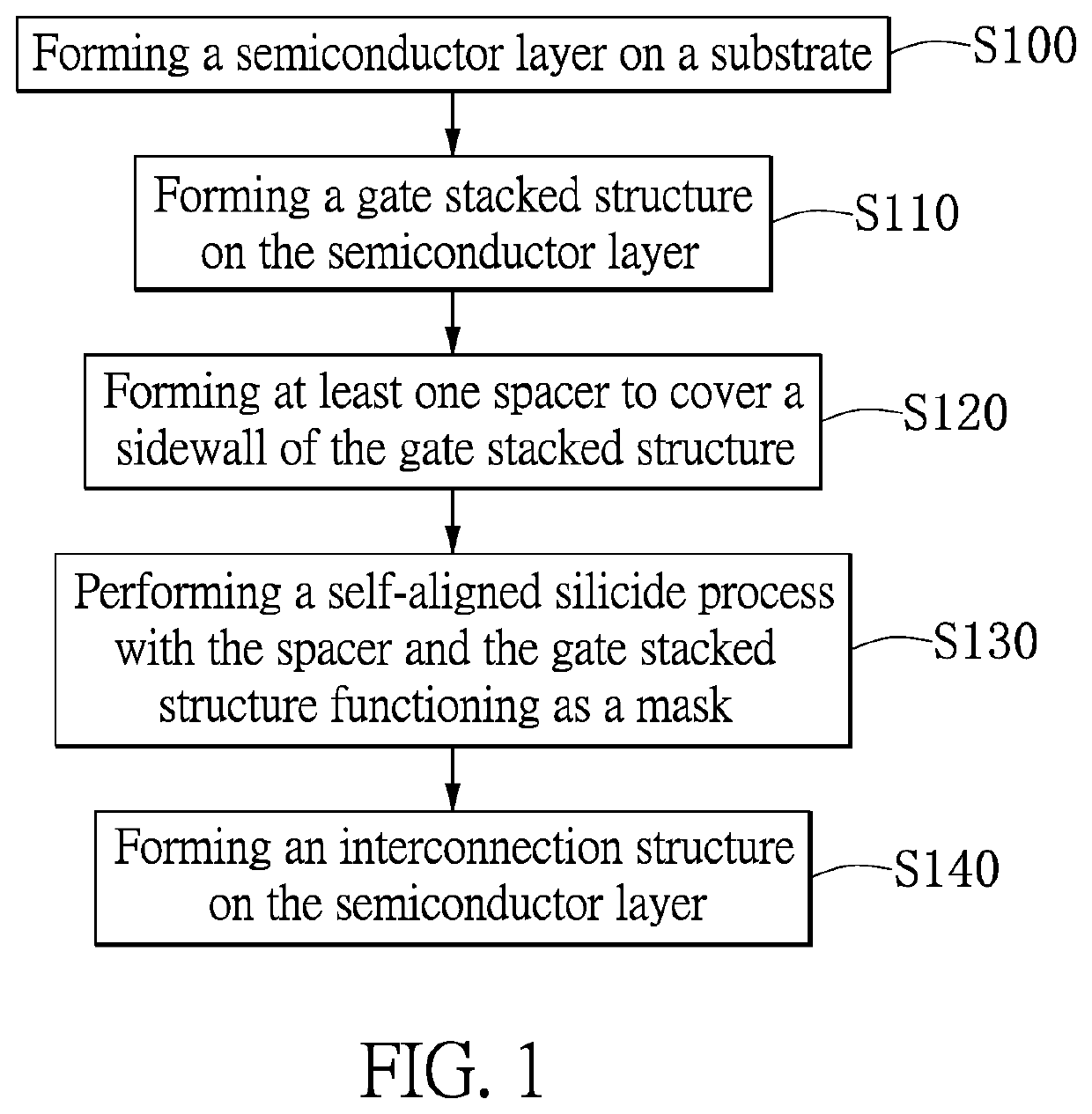
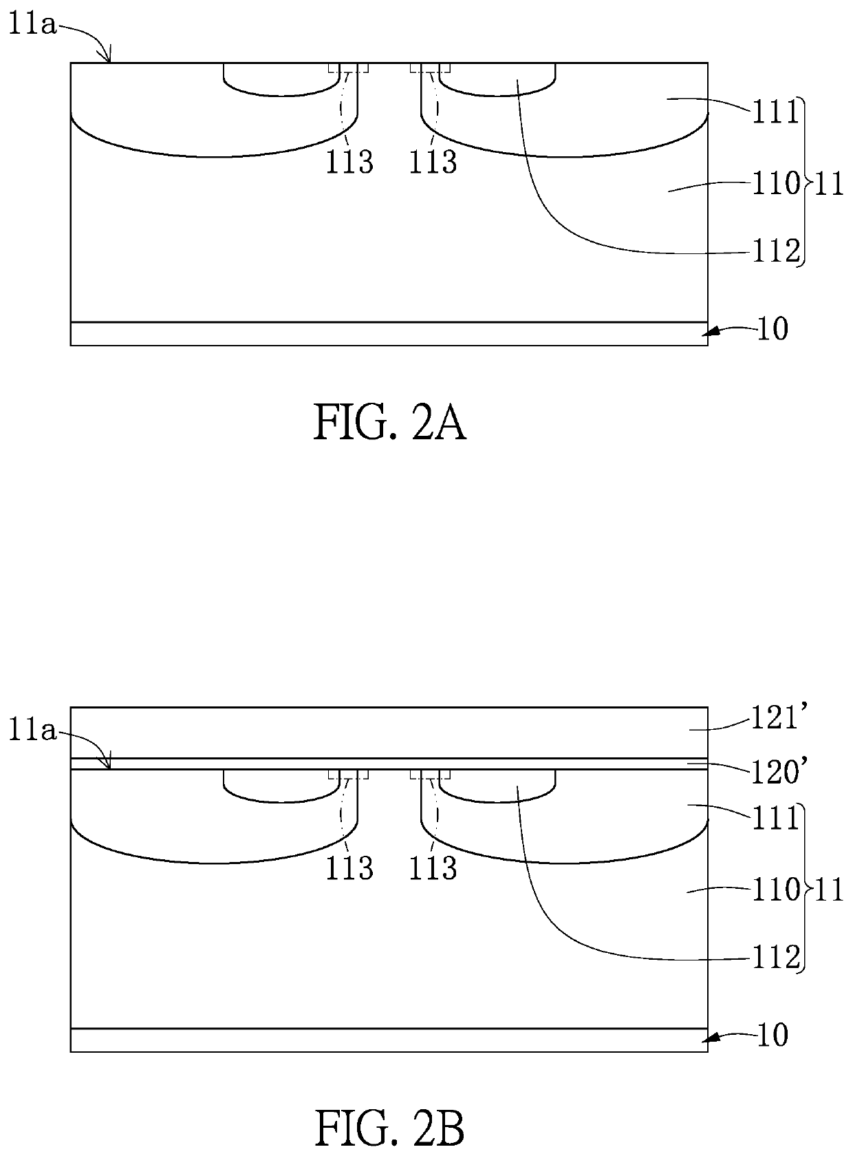
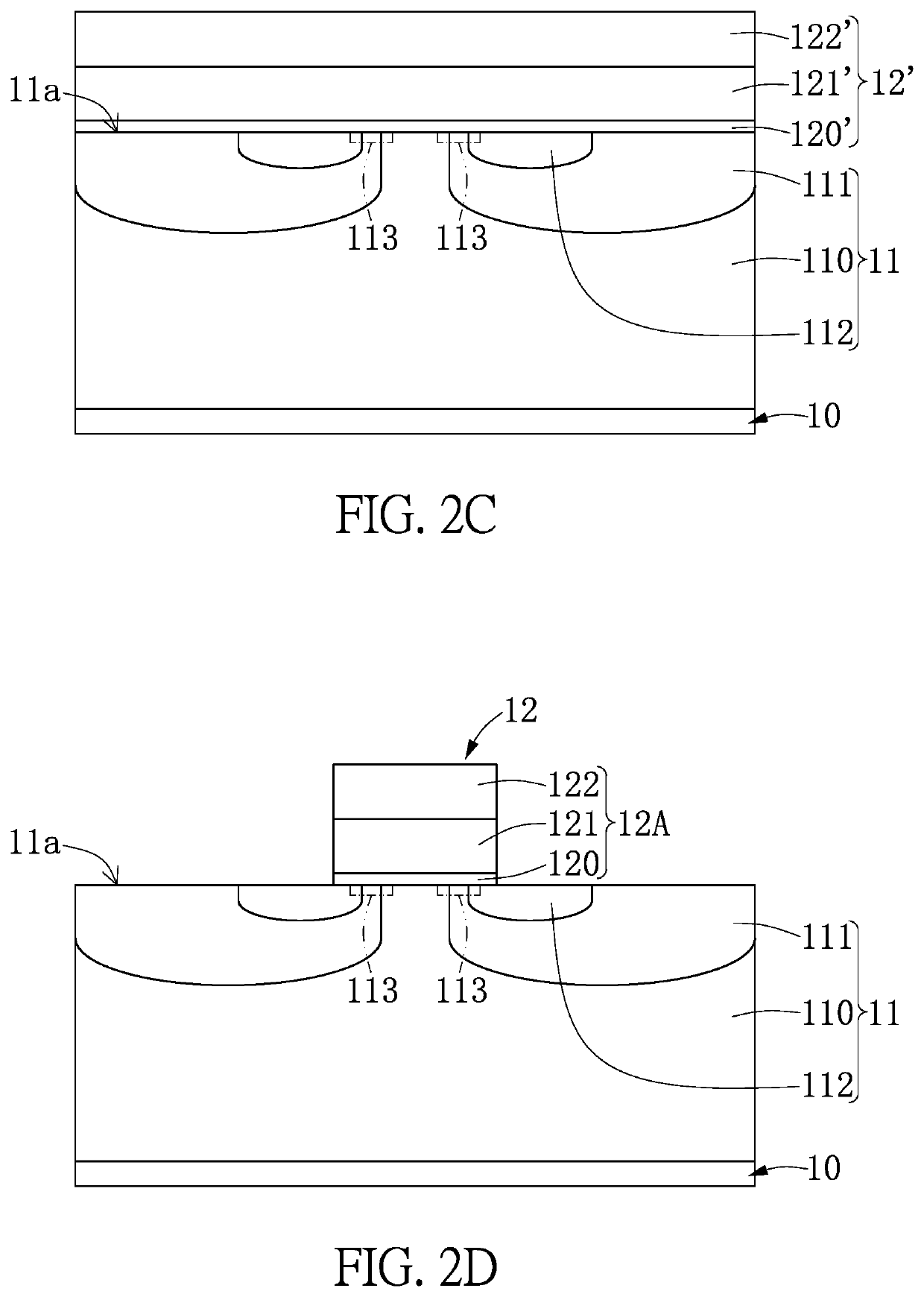
[0028]The present disclosure is more particularly described in the following examples that are intended as illustrative only since numerous modifications and variations therein will be apparent to those skilled in the art. Like numbers in the drawings indicate like components throughout the views. As used in the description herein and throughout the claims that follow, unless the context clearly dictates otherwise, the meaning of “a”, “an”, and “the” includes plural reference, and the meaning of “in” includes “in” and “on”. Titles or subtitles can be used herein for the convenience of a reader, which shall have no influence on the scope of the present disclosure.

[0029]The terms used herein generally have their ordinary meanings in the art. In the case of conflict, the present document, including any definitions given herein, will prevail. The same thing can be expressed in more than one way. Alternative language and synonyms can be used for any term(s) discussed herein, and no speci...


PUM

PropertyMeasurementUnit
thicknessaaaaaaaaaa
conductiveaaaaaaaaaa
thicknessaaaaaaaaaa

Abstract

A semiconductor power device and a manufacturing method thereof are provided. In the manufacturing method, before the self-aligned silicide process is performed, a gate stacked structure and a spacer are formed on a semiconductor layer having a body region and a source region. The spacer defines a portion of the source region for forming a silicide layer. Subsequently, the self-aligned silicide process is performed with the gate stacked structure and the spacer functioning as a mask to form the silicide layer at the defined portion of the source region. Thereafter, an interconnection structure including an interlayer dielectric layer and a source conductive layer is formed on the semiconductor layer. The source conductive layer is electrically connected to the source region. The silicide layer extends toward the gate stacked structure from a position under the source conductive layer to another position under the interlayer dielectric layer.

Description

CROSS-REFERENCE TO RELATED PATENT APPLICATION[0001]This application claims the benefit of priority to Taiwan Patent Application No. 107124782, filed on Jul. 18, 2018. The entire content of the above identified application is incorporated herein by reference.[0002]Some references, which may include patents, patent applications and various publications, may be cited and discussed in the description of this disclosure. The citation and / or discussion of such references is provided merely to clarify the description of the present disclosure and is not an admission that any such reference is “prior art” to the disclosure described herein. All references cited and discussed in this specification are incorporated herein by reference in their entireties and to the same extent as if each reference was individually incorporated by reference.FIELD OF THE DISCLOSURE[0003]The present disclosure relates to a semiconductor power device and a manufacturing method thereof, and more particularly to a ...

Claims


Application Information

Patent Timeline
Patent Type & Authority Patents(United States)
IPC IPC(8): H01L29/66H01L29/06H01L21/768
CPCH01L29/66719H01L29/665H01L29/6656H01L21/76838H01L29/0696H01L29/1608H01L29/401H01L29/41741H01L29/4916H01L29/66068H01L29/7802H01L29/7811
Inventor TANG, SUNG-NIENCHEN, HO-TAIHSU, HSIU-WEN
Owner SUPER GROUP SEMICON
Features
  • R&D
  • Intellectual Property
  • Life Sciences
  • Materials
  • Tech Scout
  • Unparalleled Data Quality
  • Higher Quality Content
  • 60% Fewer Hallucinations
Learn More