Silicon carbide semiconductor device and manufacturing method of same

a technology of silicon carbide and semiconductors, applied in the direction of semiconductor devices, basic electric elements, electrical equipment, etc., can solve the problems of gate insulating film breakdown, electric field concentration at the bottom of the trench, and the effect of reducing on resistance, excessive electric field concentration, and prolonging the depletion layer

Active Publication Date: 2021-02-11
MITSUBISHI ELECTRIC CORP
View PDF0 Cites 0 Cited by
  • Summary
  • Abstract
  • Description
  • Claims
  • Application Information

AI Technical Summary

Benefits of technology

[0013]According to the present invention, the extension of a depletion layer from the vicinity of the border between the trench and the protective layer is suppressed by the first low-resistance layer. Further, the extension of the depletion layer can be further suppressed by the second low-resistance layer having a relatively high impurity concentration. On-resistance can be reduced by reducing the JFET resistance with the first low-resistance layer and the second low-resistance layer. Since the second low-resistance

Problems solved by technology

In the trench gate semiconductor devices, there is a problem that electric field concentration occurs at the bottom of the trench when a high voltage is applied in an off-state of the semiconductor device.
In particular, in the trench gate silicon carbide semiconductor devices, SiC has high dielectric breakdown strength, and hence gate insulating film breakdown, due to the electric field concentration at the bottom of the trench, is likely to occur before avalanche breakdown in the drift layer.
Therefore, in the trench gate silicon carbide semiconductor devices, the electric field concentration at the bottom of the trench is likely to be a problem.
In such a structure, however, there is a problem that a junction field effect transistor (JFET) resistance to a current flowing t

Method used


Image

  • Silicon carbide semiconductor device and manufacturing method of same
  • Silicon carbide semiconductor device and manufacturing method of same
  • Silicon carbide semiconductor device and manufacturing method of same

Examples


first embodiment

[0041](Overview of Configuration)

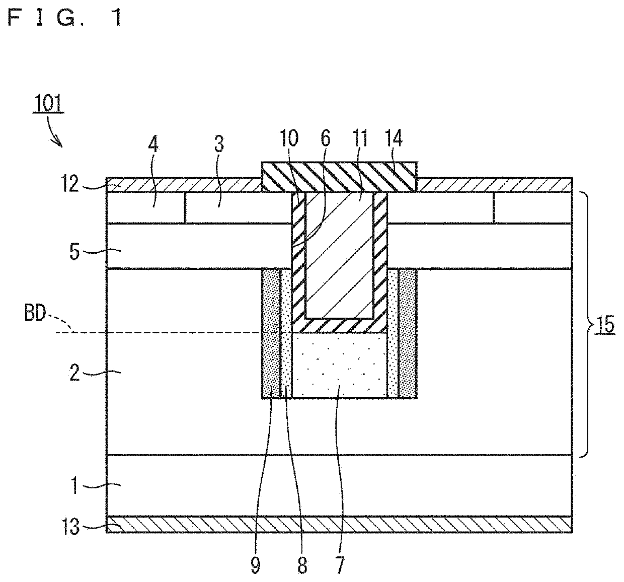
[0042]FIG. 1 is a partial cross-sectional view schematically illustrating a structure of a cell of a MOSFET 101 (silicon carbide semiconductor device) according to a first embodiment. The MOSFET 101 (silicon carbide semiconductor device) has a semiconductor layer 15, a gate insulating film 10, and a gate electrode 11, and the MOSFET 101 may further have a substrate 1 (semiconductor substrate), a source electrode 12, a drain electrode 13, and an interlayer insulating film 14. The semiconductor layer 15 has a drift layer 2, a body region 5, a source region 3, at least one protective layer 7, at least one first low-resistance layer 8, and at least one second low-resistance layer 9. The semiconductor layer 15 may further have a body contact region 4.

[0043]The drift layer 2 is made of silicon carbide. The drift layer 2 has a first conductivity type. The first conductivity type is either an n-type or a p-type, and is preferably an n-type. The body region 5...

second embodiment

Modification of Second Embodiment

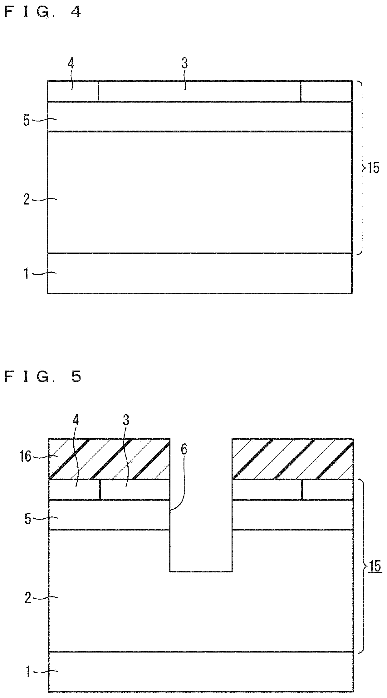
[0113]The first low-resistance layer 8 and the second low-resistance layer 9 may be formed by vertical ion implantation into the surface of the semiconductor layer 15 or by epitaxial growth. For example, after the drift layer 2 is formed according to the manufacturing method of the first embodiment, as illustrated in FIG. 3, the second low-resistance layer 9 is formed by ion implantation or epitaxial growth. The first low-resistance layer 8 is formed thereon by ion implantation or epitaxial growth. In this ion implantation or epitaxial growth, the first low-resistance layer 8 and the second low-resistance layer 9 may be formed locally by using a mask partially having an opening. Thereafter, the body region 5, the source region 3, and the body contact region 4 are formed by the same method as in the first embodiment. Then, the trench 6 is formed to contact the side surface of the first low-resistance layer 8, and the protective layer 7 is formed to co...

third embodiment

[0117](Configuration)

[0118]FIG. 22 is a partial cross-sectional view schematically illustrating a structure of a cell of a MOSFET 103 (silicon carbide semiconductor device) according to a third embodiment. The differences between the MOSFET 103 and the MOSFET 101 (FIG. 1: first embodiment) are: the configurations of a first low-resistance layer 8 and a second low-resistance layer 9 and methods of forming them; and the fact that a third low-resistance layer 17 is formed, and hence the differences will be mainly described below.

[0119]Also in the MOSFET 103, the first low-resistance layer 8 covers the side surface of the trench 6 below the body region 5, similarly to the MOSFET 101. The second low-resistance layer 9 is formed to contact the side surface of the first low-resistance layer 8.

[0120]In the MOSFET 103, the third low-resistance layer 17 is further provided as part of the semiconductor layer 15 in addition to the first low-resistance layer 8 and the second low-resistance layer...


PUM


Abstract

A drift layer made of silicon carbide has a first conductivity type. A body region on the drift layer has a second conductivity type. A source region on the body region has the first conductivity type. A gate insulating film is on each inner wall of at least one trench. A protective layer has at least a portion below the trench, is in contact with the drift layer, and has the second conductivity type. A first low-resistance layer is in contact with the trench and the protective layer, straddles a border between the trench and the protective layer in the depth direction, has the first conductivity type, and has a higher impurity concentration than the drift layer. A second low-resistance layer is in contact with the first low-resistance layer, is away from the trench, has the first conductivity type, and has a higher impurity concentration than the first low-resistance layer.

Description

TECHNICAL FIELD[0001]The present invention relates to a silicon carbide semiconductor device having a trench gate and a manufacturing method of the same.BACKGROUND ART[0002]As power switching elements, insulated gate semiconductor devices, such as metal oxide semiconductor field effect transistors (MOSFETs) and insulated gate bipolar transistors (IGBTs), are widely used. The on-state of an insulated gate semiconductor device is obtained by forming a channel in a body region by applying a voltage higher than or equal to a threshold voltage to a gate electrode. Among such insulated gate semiconductor devices, a trench gate type has a trench reaching a drift layer from the surface of a semiconductor layer, and the body region of the side surface of the trench is used as the channel. With this channel structure, a channel width density can be improved. Therefore, a cell pitch can be reduced, whereby device performance can be improved.[0003]On the other hand, as next-generation semicondu...

Claims


Application Information

Patent Timeline
IPC IPC(8): H01L29/78H01L29/10H01L29/16
CPCH01L29/7813H01L29/1608H01L29/1095H01L29/0623H01L29/0878H01L29/66068H01L29/4236H01L21/047
Inventor TANAKA, RINASUGAWARA, KATSUTOSHIFUKUI, YUTAKAHATTA, HIDEYUKIMIYATA, YUSUKE
Owner MITSUBISHI ELECTRIC CORP
Why Eureka
Try Eureka