Semiconductor device having a drain drift-region in contact with the body region
a technology of sinking region and sinking device, which is applied in the direction of sinking device, basic electric element, electrical apparatus, etc., can solve the problems of difficult to reduce on-resistance, and achieve the effect of suppressing hot-carrier degradation, reducing on-resistance, and high drain breakdown voltag
- Summary
- Abstract
- Description
- Claims
- Application Information
AI Technical Summary
Benefits of technology
Problems solved by technology
Method used
Image

Examples
first embodiment
[0035]Now, a semiconductor device and a method of manufacturing the same according to the first embodiment of the present invention are described.
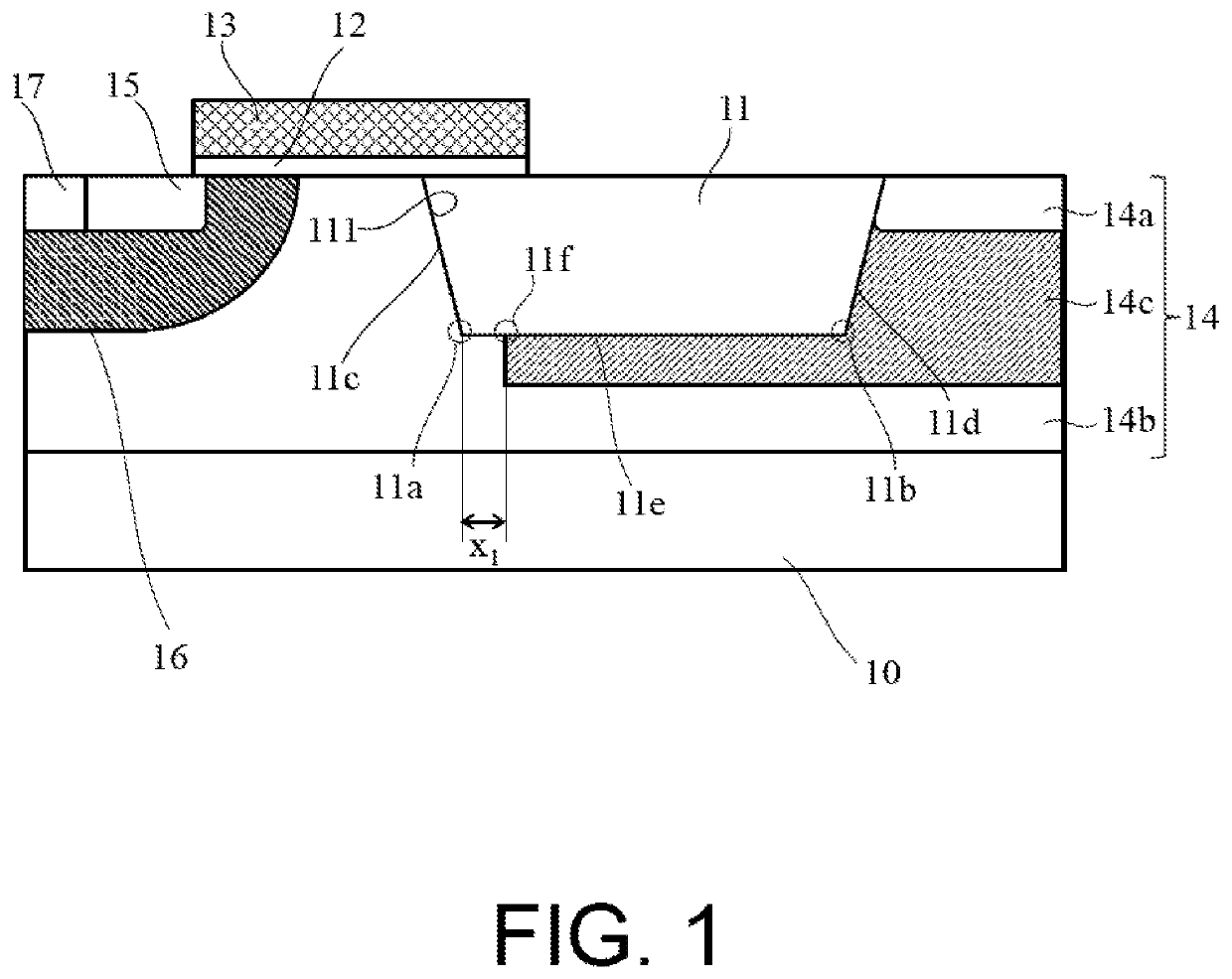
[0036]FIG. 1 is a cross-sectional view of a semiconductor device 1 according to the first embodiment of the present invention.
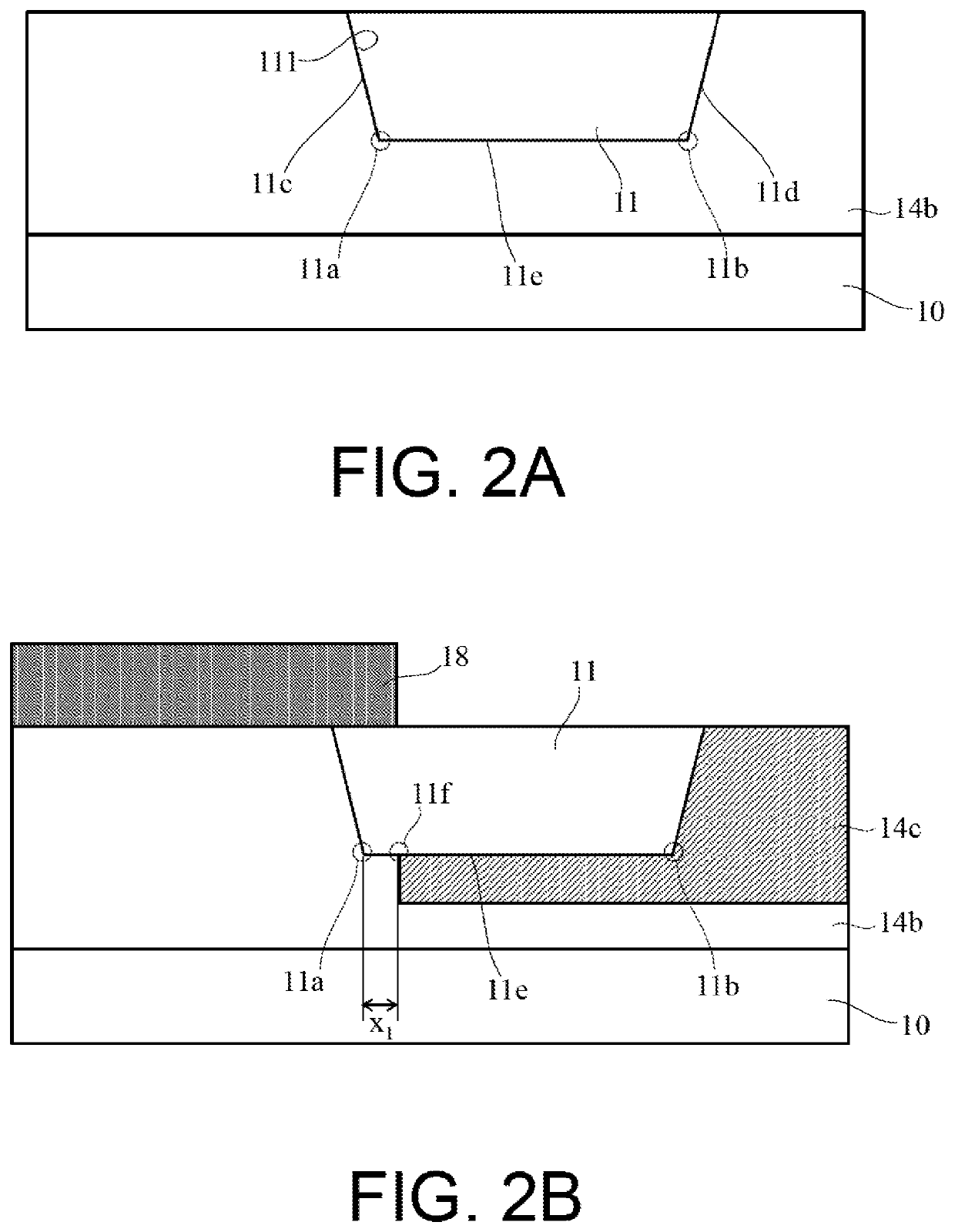
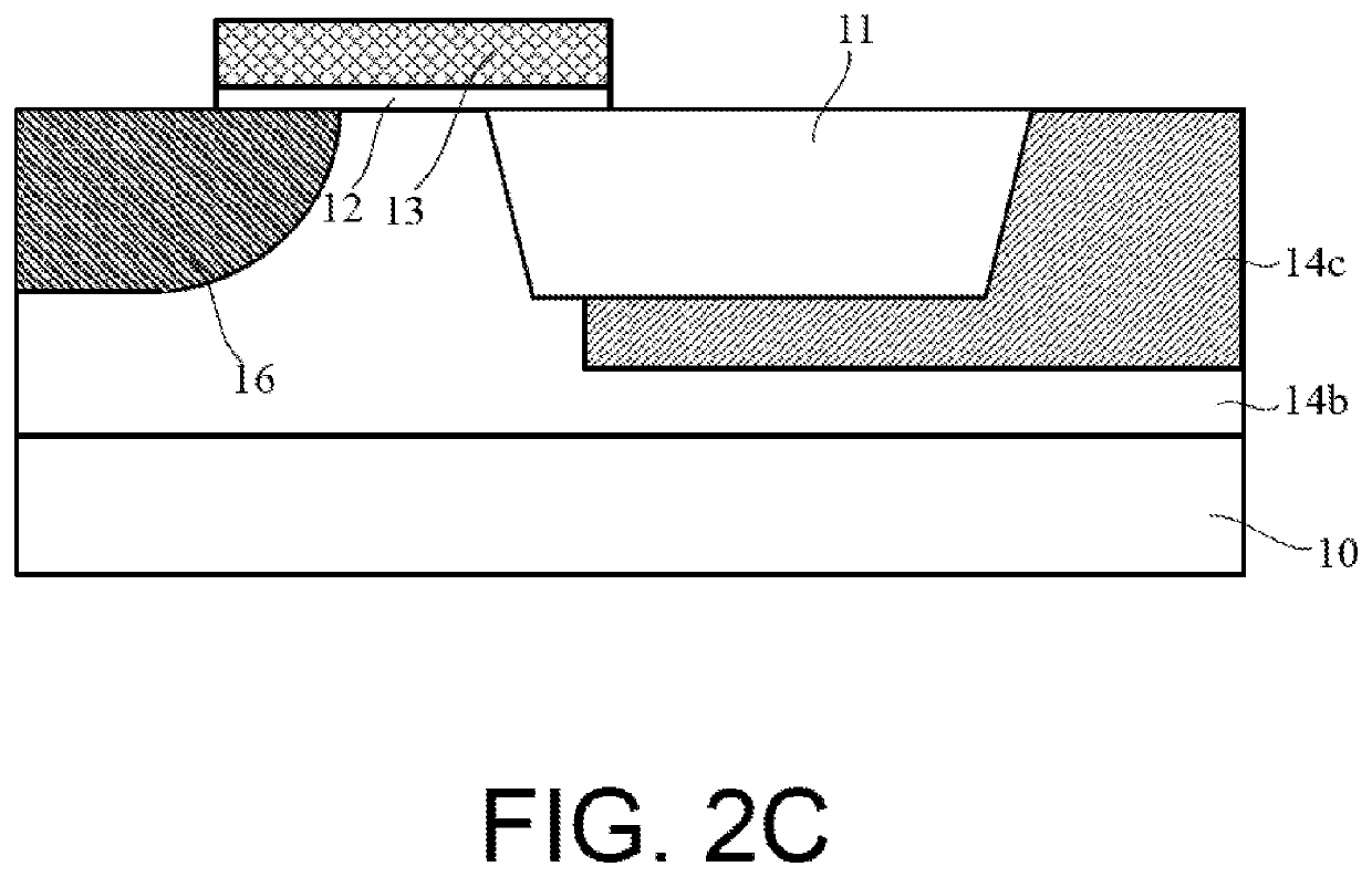
[0037]The semiconductor device 1 according to the first embodiment is formed on a semiconductor substrate 10 made of p-type silicon, for example, and includes an n-type drain region 14 and an n-type source region 15, a p-type body region 16 formed between the drain region 14 and the source region 15, a p-type body contact region 17 formed on the body region 16, a gate insulating film 12, and a gate electrode 13. The drain region 14 includes a high-concentration drain region 14a, a first drain drift-region 14b, and a second drain drift-region 14c. Moreover, a trench 111 is formed in the drain region 14, and an STI insulating film 11 (thick insulating film) having a thickness that is larger than that of the gate insul...
second embodiment
[0055]Now, a semiconductor device and a method of manufacturing the same according to a second embodiment of the present invention are described.
[0056]FIG. 3 is a cross-sectional view of a semiconductor device 2 according to the second embodiment of the present invention.
[0057]The semiconductor device 2 according to the second embodiment is formed on a semiconductor substrate 20 made of p-type silicon, for example, and includes an n-type drain region 24 and an n-type source region 25, a p-type body region 26 formed between the drain region 24 and the source region 25, a p-type body contact region 27 formed on the body region 26, a gate insulating film 22, and a gate electrode 23. The drain region 24 includes a high-concentration drain region 24a, a first drain drift-region 24b, and a second drain drift-region 24c. Moreover, a trench 211 is formed in the drain region 24, and an STI insulating film 21 having a thickness that is larger than that of the gate insulating film 22 is formed...
third embodiment
[0072]Now, a semiconductor device and a method of manufacturing the same according to a third embodiment of the present invention are described.
[0073]FIG. 5 is a cross-sectional view of a semiconductor device 3 according to the third embodiment of the present invention.
[0074]The semiconductor device 3 according to the third embodiment is formed on a semiconductor substrate 30 made of p-type silicon, for example, and includes an n-type drain region 34 and an n-type source region 35, a p-type body region 36 formed between the drain region 34 and the source region 35, a p-type body contact region 37 formed on the body region 36, a gate insulating film 32, and a gate electrode 33. The drain region 34 includes, in addition to a high-concentration drain region 34a, a first drain drift-region 34b, and a second drain drift-region 34c, a surface drain drift-region 34d. A trench 311 is formed in the drain region 34, and an STI insulating film 31 having a thickness that is larger than that of ...
PUM
| Property | Measurement | Unit |
|---|---|---|
| interior angle | aaaaa | aaaaa |
| thickness | aaaaa | aaaaa |
| inclination angle | aaaaa | aaaaa |
Abstract
Description
Claims
Application Information
 - R&D
- Intellectual Property
- Life Sciences
- Materials
- Tech Scout
- Unparalleled Data Quality
- Higher Quality Content
- 60% Fewer Hallucinations
Browse by: Latest US Patents, China's latest patents, Technical Efficacy Thesaurus, Application Domain, Technology Topic, Popular Technical Reports.
© 2025 PatSnap. All rights reserved.Legal|Privacy policy|Modern Slavery Act Transparency Statement|Sitemap|About US| Contact US: help@patsnap.com