Method for producing semiconductor device
a technology of nitride and semiconductor, applied in the direction of semiconductor devices, basic electric elements, electrical equipment, etc., can solve the problems of reducing the threshold voltage of the gate channel, etching damage on the side surface of the exposed trench, and reducing the acceptor concentration of the exposed side surface, so as to achieve the effect of reducing the resistance of the channel and reducing the on resistan
- Summary
- Abstract
- Description
- Claims
- Application Information
AI Technical Summary
Benefits of technology
Problems solved by technology
Method used
Image

Examples
first embodiment
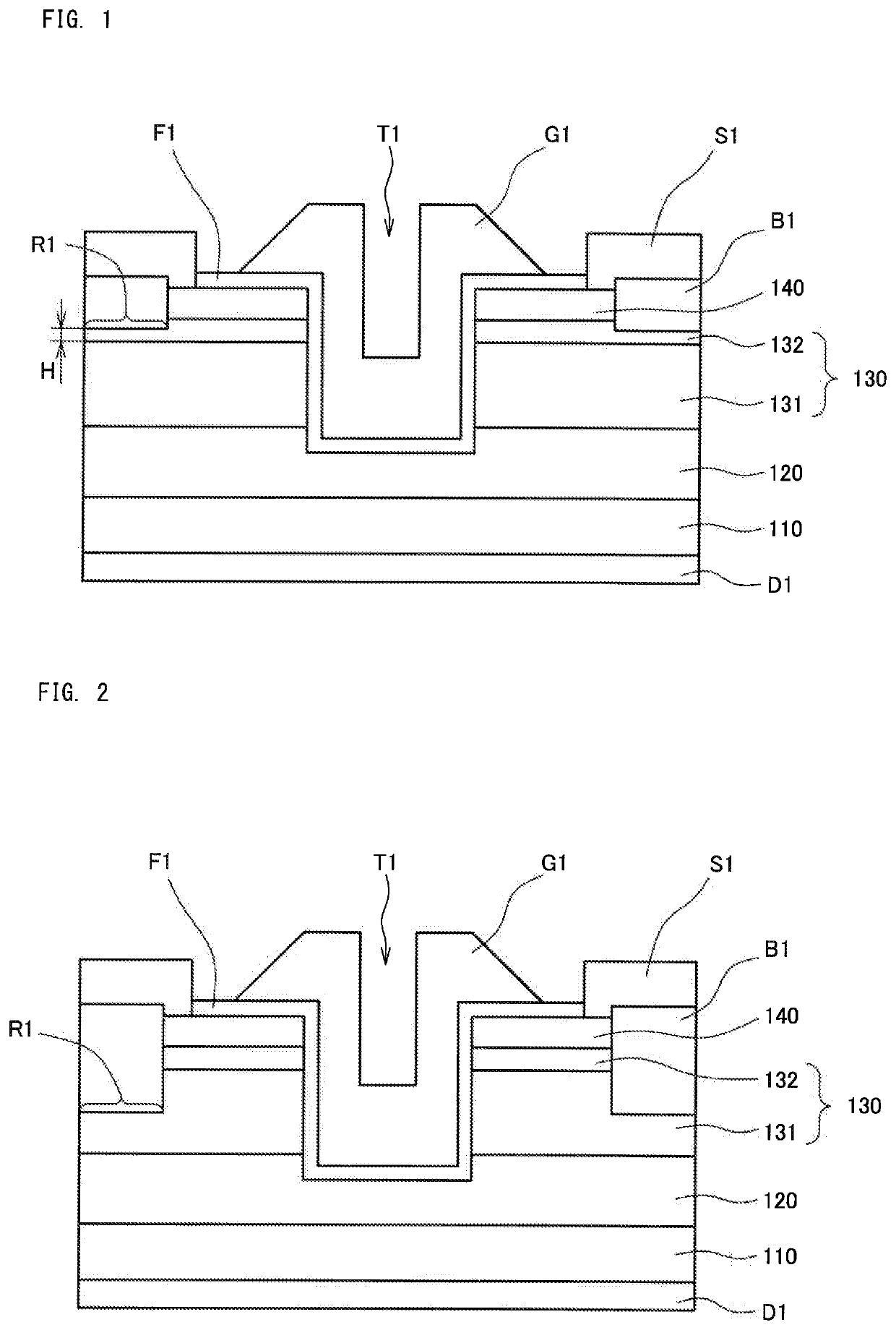
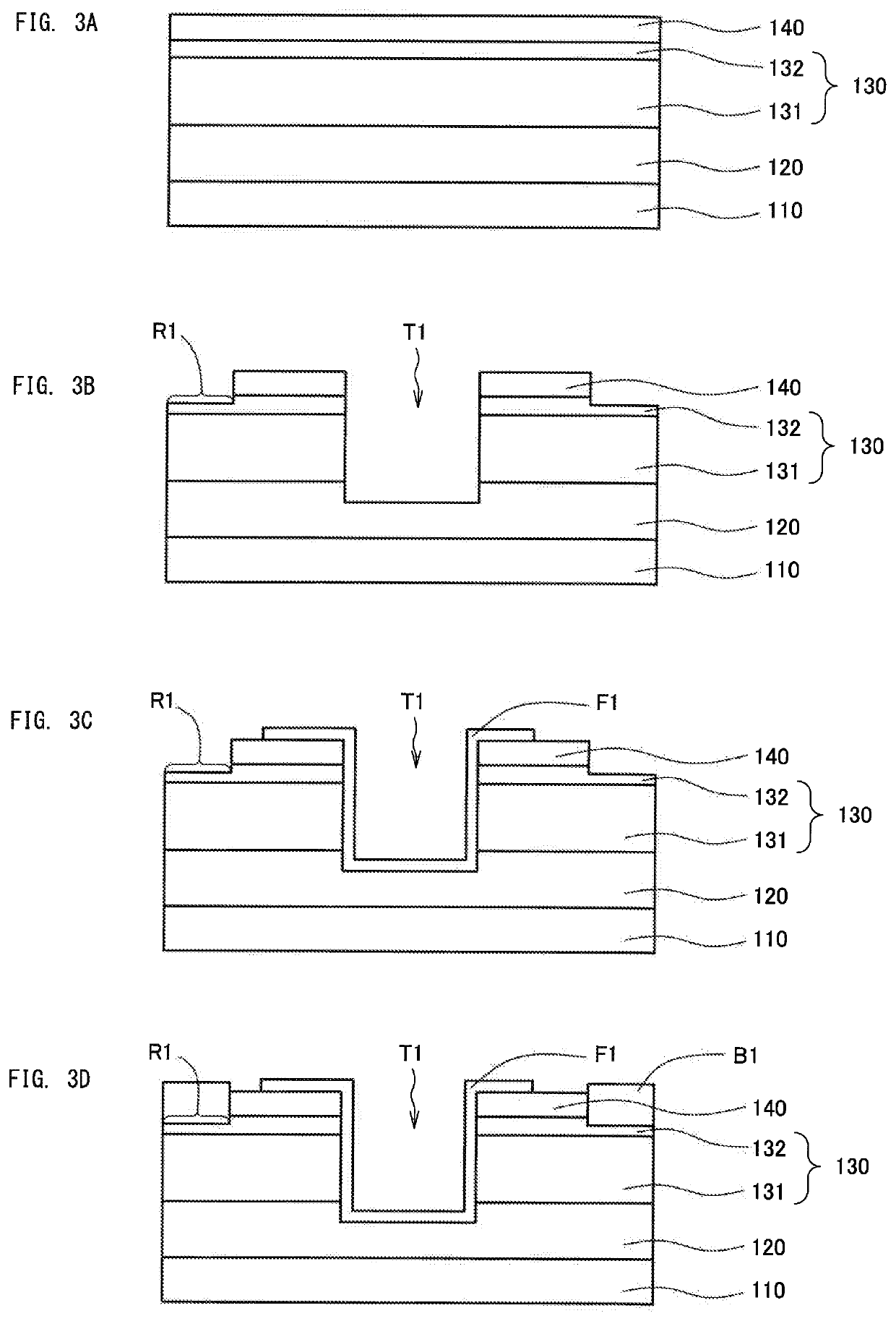
[0024]FIG. 1 shows the structure of a semiconductor device according to a first embodiment. As shown in FIG. 1, the semiconductor device according to the first embodiment is a vertical MISFET having a trench gate structure, which includes a substrate 110, a first n-type layer 120, a p-type layer 130, a second n-type layer 140, a trench T1, a recess R1, a gate insulating film F1, a gate electrode G1, a source electrode S1, a body electrode B1, and a drain electrode D1.
[0025]The substrate 110 is a flat plate-shaped substrate made of Si-doped n-GaN having a c-plane main surface. The substrate 110 has a thickness of, for example, 300 μm and a Si concentration of, for example, 1×10¹⁸ / cm3. Any conductive material other than n-GaN may be used as a substrate for growing Group III nitride semiconductor. For example, ZnO or Si may be used. However, in terms of lattice matching, a GaN substrate is preferably used as in the present embodiment. Si is used as an n-type impurity in the first embod...
second embodiment
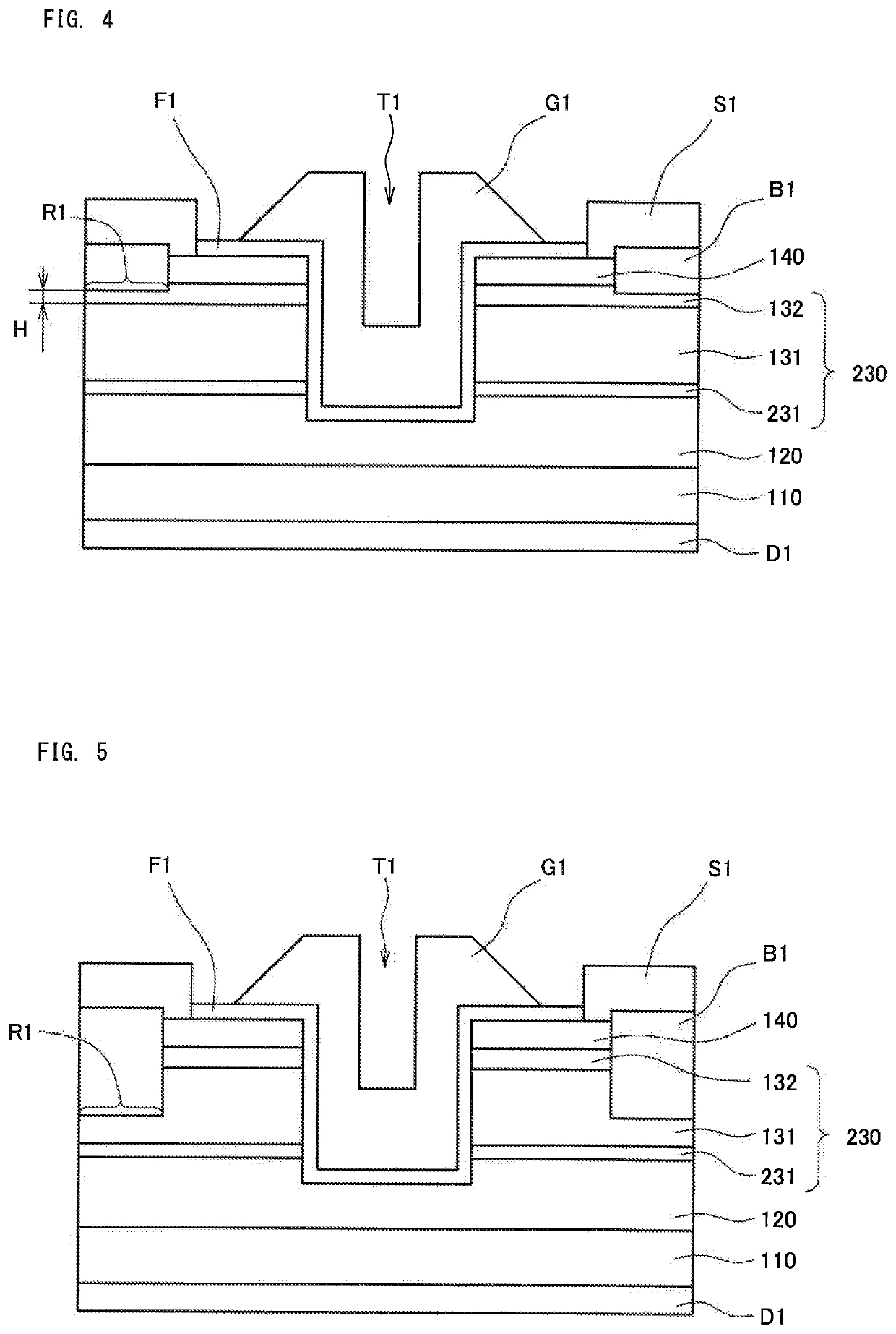
[0059]FIG. 4 shows the structure of a semiconductor device according to a second embodiment. The semiconductor device according to the second embodiment has a structure in which a third p-type layer 231 is further formed between the first n-type layer 120 and the first p-type layer 131 in the semiconductor device according to the first embodiment. That is, the p-type layer 130 is substituted by a p-type layer 230 having a three-layer structure in which a third p-type layer 231, a first p-type layer 131, and a second p-type layer 132 are sequentially deposited. Other structure is the same as that of the semiconductor device according to the first embodiment.
[0060]The third p-type layer 231 is the bottom layer of a plurality of layers constituting the p-type layer 230, and is in contact with the first n-type layer 120. The third p-type layer 231 has a Mg concentration higher than the Mg concentration of the first p-type layer 131 and not more than the Mg concentration of the second p-...
third embodiment
[0064]FIG. 7 shows the structure of a semiconductor device according a third embodiment. In the semiconductor device according to the third embodiment, the p-type layer 130, the recess R1, and the body electrode B1 in the first embodiment are respectively substituted by a p-type layer 330, a recess R2, and a body electrode 32. Other structure is the same as that of the semiconductor device according to the first embodiment.
[0065]The p-type layer 330 is a Mg-doped p-GaN layer deposited on the first n-type layer 120. The p-type layer 330 has a two-layer structure in which a first p-type layer 331 and a second p-type layer 332 are sequentially deposited.
[0066]The first p-type layer 331 has a Mg concentration higher than the Mg concentration of the second p-type layer 332, and is in contact with the first n-type layer 120. The first p-type layer 331 is provided to increase the threshold voltage. The first p-type layer 331 is provided to minimize the expansion of the depletion layer to t...
PUM
| Property | Measurement | Unit |
|---|---|---|
| thickness | aaaaa | aaaaa |
| thickness | aaaaa | aaaaa |
| total thickness | aaaaa | aaaaa |
Abstract
Description
Claims
Application Information
 - R&D
- Intellectual Property
- Life Sciences
- Materials
- Tech Scout
- Unparalleled Data Quality
- Higher Quality Content
- 60% Fewer Hallucinations
Browse by: Latest US Patents, China's latest patents, Technical Efficacy Thesaurus, Application Domain, Technology Topic, Popular Technical Reports.
© 2025 PatSnap. All rights reserved.Legal|Privacy policy|Modern Slavery Act Transparency Statement|Sitemap|About US| Contact US: help@patsnap.com