Semiconductor device having circuit board to which contact part is bonded

a technology of semiconductor devices and contact parts, which is applied in the direction of basic electric elements, manufacturing tools, and solvents, etc., can solve the problems of deteriorating thickness of bonding materials at the bonding portion, and deteriorating reliability of semiconductor devices

Active Publication Date: 2021-08-31
FUJI ELECTRIC CO LTD
View PDF14 Cites 0 Cited by
  • Summary
  • Abstract
  • Description
  • Claims
  • Application Information

AI Technical Summary

Benefits of technology

[0044]The embodiments discussed herein achieve reduction of the rising of bonding material into hollow holes of contact parts and achieve bonding of external connection terminals to circuit boards without fail. Thus, the deterioration of the reliability of the semiconductor device is prevented.

Problems solved by technology

However, if the amount of bonding material such as solder used for bonding the circuit board of the multilayer substrate and the contact part is small, the thickness of the bonding material is not ensured at the bonding portion.
If the bonding strength of the contact part with respect to the circuit board is reduced, the reliability of the semiconductor device could be deteriorated.
As a result, the reliability of the semiconductor device could be deteriorated.

Method used


Image

  • Semiconductor device having circuit board to which contact part is bonded
  • Semiconductor device having circuit board to which contact part is bonded
  • Semiconductor device having circuit board to which contact part is bonded

Examples


first embodiment

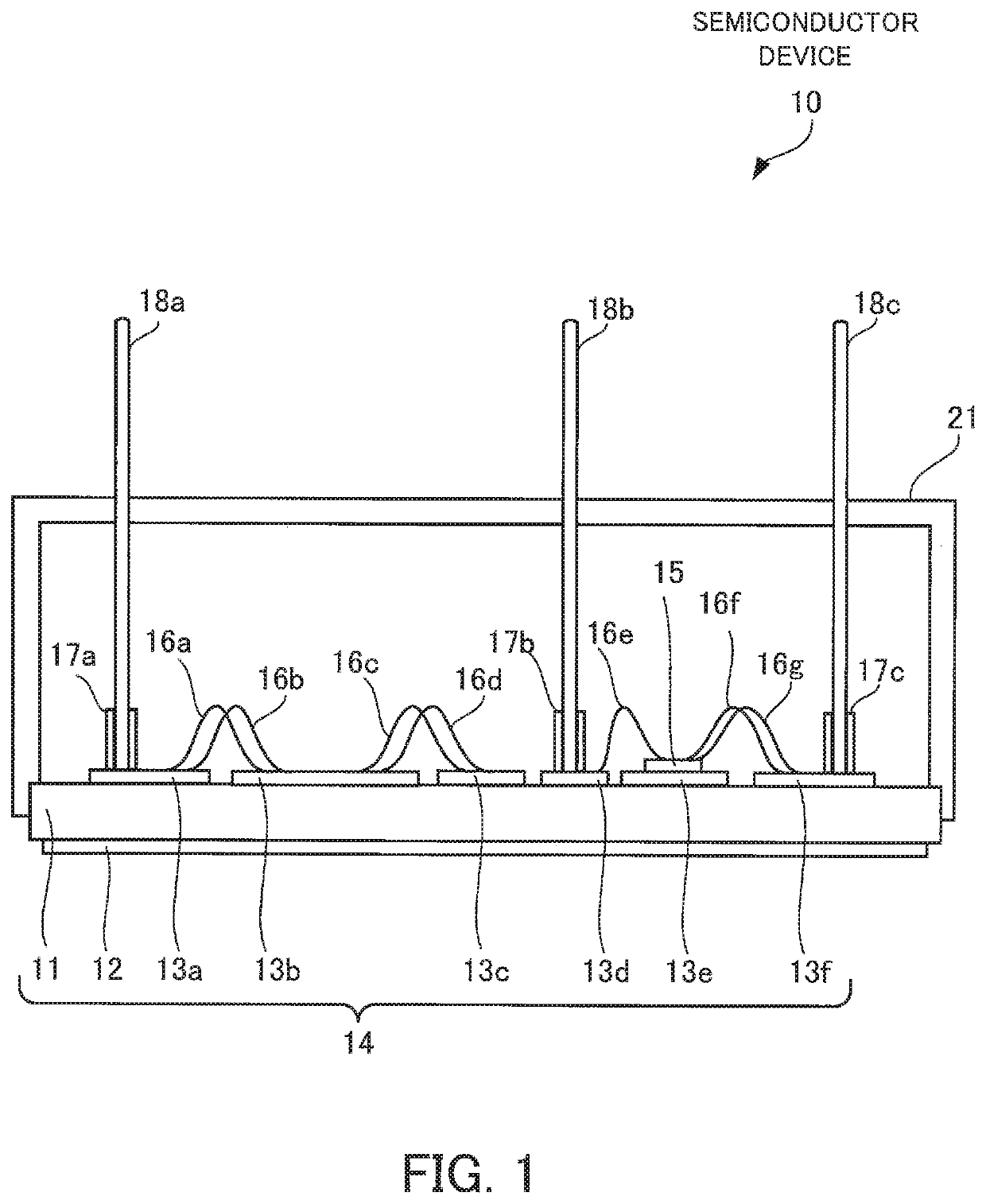
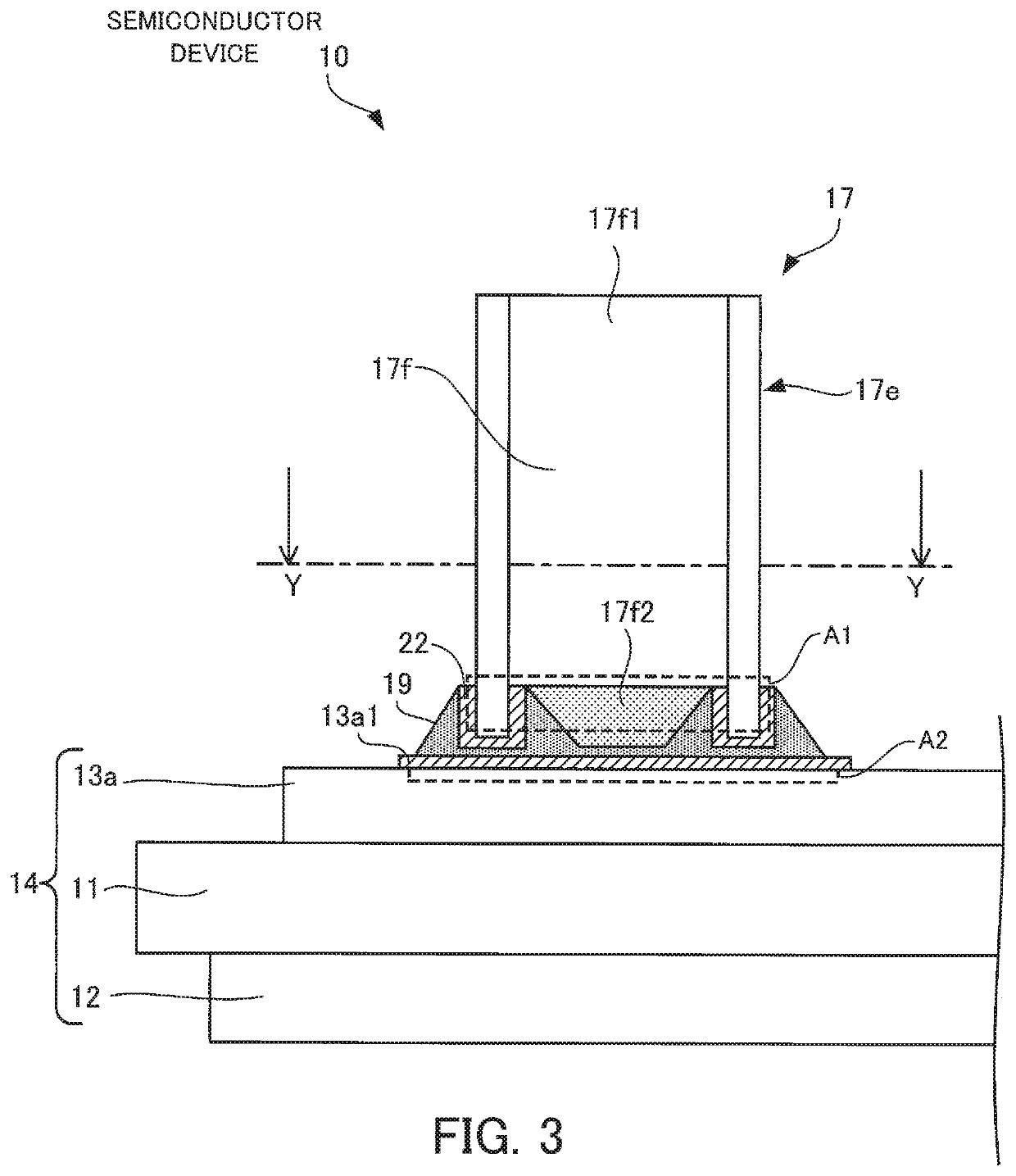
[0017]First, a semiconductor device according to a first embodiment will be described with reference to FIG. 1. FIG. is a sectional side view of a semiconductor device according to a first embodiment. As illustrated in FIG. 1, this semiconductor device 10 includes a multilayer substrate 14, semiconductor elements 15 and contact parts 17a to 17c arranged on the front surface of the multilayer substrate 14, and external connection terminals 18a to 18c attached to the contact parts 17a to 17c, respectively. The plurality of semiconductor elements 15 are arranged on the multilayer substrate 14 while only one of the semiconductor elements 15 is illustrated in FIG. 1. The semiconductor element 15 may be arranged at a different position other than the position illustrated in FIG. 1. A case 21 is bonded to the outer periphery of the multilayer substrate 14. Thus, the semiconductor elements 15, the contact parts 17a to 17c, the external connection terminals 18a to 18c, etc. are stored in the...

second embodiment

[0034]A semiconductor device according to a second embodiment has the same structure as that of the semiconductor device 10 illustrated in FIG. 1. However, the plating areas of the first plating material and the second plating material of the semiconductor device according to the second embodiment are different from those of the semiconductor device 10 according to the first embodiment. In addition, specific materials are used as the first plating material, the second plating material, and the bonding material. In addition, contact parts that are different from those according to the first embodiment are used.

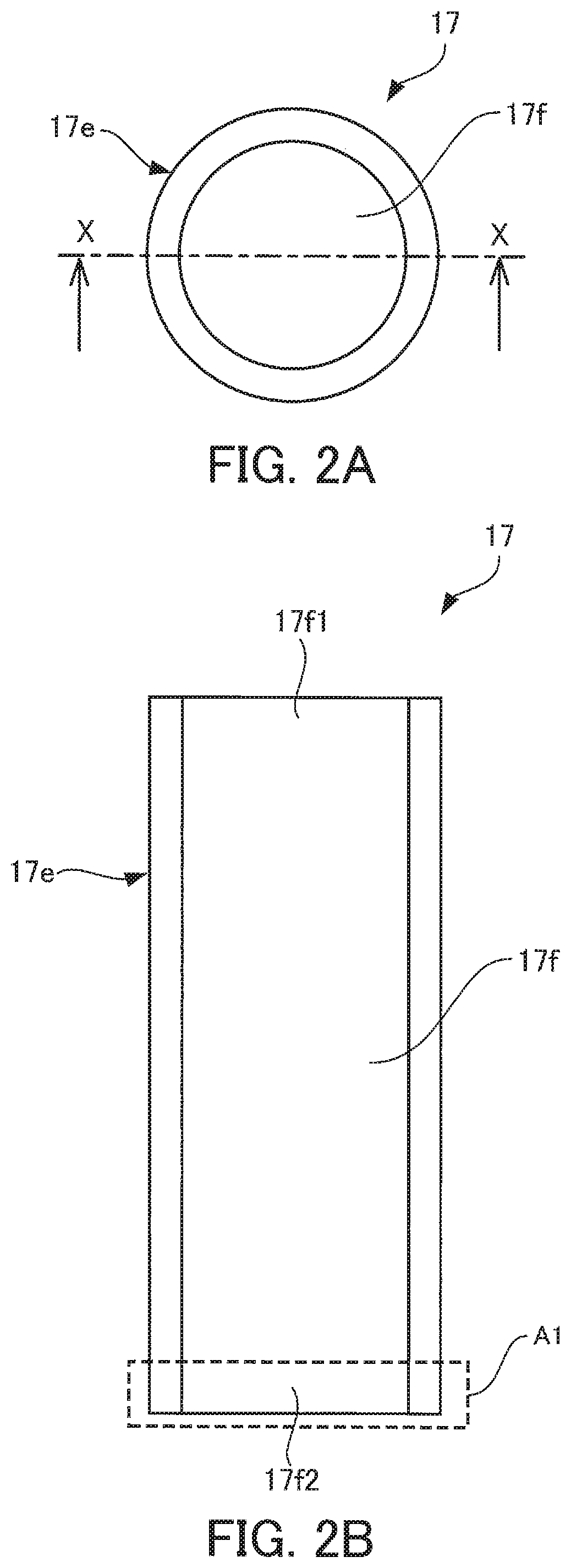
[0035]First, a contact part different from that according to the first embodiment will be described with reference to FIGS. 5A and 5B. FIGS. 5A and 5B illustrate a contact part according to the second embodiment. FIG. 5A is a plan view of an individual contact part 27. FIG. 5B is a sectional view taken along an alternate long and short dash line X-X in FIG. 5A. As in the semico...


PUM

PropertyMeasurementUnit
thicknessaaaaaaaaaa
thicknessaaaaaaaaaa
thicknessaaaaaaaaaa

Abstract

A semiconductor device includes: a multilayer substrate which includes a circuit board and an insulating plate on which the circuit board is formed; and a contact part having a cylindrical hollow hole therein and an open end bonded to a bonding area on the front surface of the circuit board via bonding material. In the case of this semiconductor device, wettability of a contact area of the contact part with respect to the bonding material is approximately equal to wettability of at least the bonding area of the circuit board with respect to the bonding material. Thus, the rising of the bonding material into the hollow hole of the contact part during heating performed when the contact part is bonded to the circuit board is reduced.

Description

CROSS-REFERENCE TO RELATED APPLICATION[0001]This application is a continuation application of International Application PCT / JP2019 / 004050 filed on Feb. 5, 2019 which designated the U.S., which claims priority to Japanese Patent Application No. 2018-049524, filed on Mar. 16, 2018, the entire contents of which are incorporated herein by reference.BACKGROUND OF THE INVENTION1. Field of the Invention[0002]The embodiments discussed herein relate to a semiconductor device.2. Background of the Related Art[0003]For example, semiconductor devices include semiconductor elements such as insulated gate bipolar transistors (IGBTs) or power metal-oxide-semiconductor field-effect transistors (MOSFETs). These semiconductor devices are used as power conversion devices, for example.[0004]A semiconductor device includes a multilayer substrate including an insulating plate and circuit boards formed on the front surface of the insulating plate. Semiconductor elements and external connection terminals ar...

Claims


Application Information

Patent Timeline
Patent Type & Authority Patents(United States)
IPC IPC(8): H01L23/00
CPCH01L24/05H01L24/45H01L2224/03462H01L2924/01028H01L2924/01029H01L2924/052B23K1/00B23K1/20H01L23/12H01L25/07H01L25/18H01R4/02H01L2224/48091H01L2224/48227H01L24/32H01L2224/32227H01L24/29H01L24/48H01L2224/73265H01L2924/19107H01L23/3735H01L23/053H01L24/49H01L2224/4912H01L2224/49113H01L25/072H01L23/49811H01L2224/45099H01L2924/00014
Inventor MARUYAMA, RIKIHIROMIYAKOSHI, MASAOKISOUTOME, MASAYUKIADACHI, KAZUYAYOKOYAMA, TAKESHI
Owner FUJI ELECTRIC CO LTD
Why Eureka
Try Eureka