Semiconductor device having trench isolation

A trench isolation, semiconductor technology, applied in the direction of semiconductor devices, semiconductor/solid-state device manufacturing, transistors, etc., can solve the problems of deterioration of the reliability of the gate insulating layer, difficulty in manufacturing high-performance transistors or flash memory, etc., to prevent reliability. worsening effect

Inactive Publication Date: 2005-02-02
RENESAS TECH CORP
View PDF3 Cites 0 Cited by
  • Summary
  • Abstract
  • Description
  • Claims
  • Application Information

AI Technical Summary

Problems solved by technology

If the gate electrode is formed to extend through the gate insulating layer on such a depressed portion, the reverse narrow channel effect will occur, and the reliability of the gate insulating layer will also deteriorate, making it difficult to manufacture high-performance transistors or flash memory.

Method used


Image

  • Semiconductor device having trench isolation
  • Semiconductor device having trench isolation
  • Semiconductor device having trench isolation

Examples


Embodiment 1

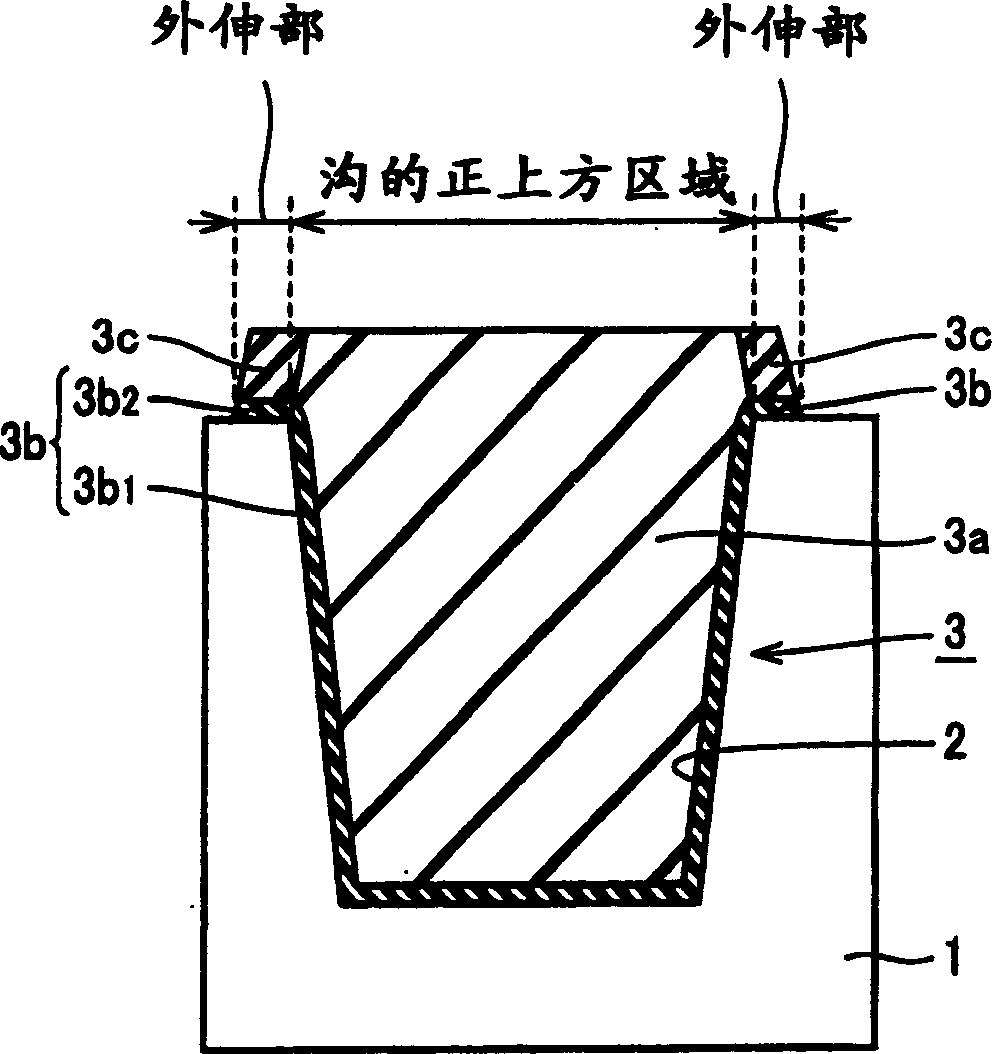
[0031] Such as figure 1 As shown, the semiconductor device of this embodiment is provided with a trench isolation portion for electrically isolating a semiconductor element from other semiconductor elements. The trench isolation portion includes, for example, a trench 2 for trench isolation formed on the surface of a semiconductor substrate 1 made of silicon, and a buried insulating layer 3 filling the trench 2 . The buried insulating layer 3 fills the trench 2 and protrudes from the surface of the semiconductor substrate 1 . The protruding portion has an overhanging portion protruding outward (in a direction parallel to the surface of the semiconductor substrate) from a region immediately above the groove 2 on the surface of the semiconductor substrate 1 . The overhanging portion has a structure in which at least two insulating layers are laminated. Furthermore, the entire upper surface of the buried insulating layer 3 is located above the surface of the semiconductor subst...

Embodiment 2

[0037] refer to figure 1 , in the semiconductor device of this embodiment, the insulating layer 3b constituting the overhang 2 and insulating layer 3c are made of different silicon oxide films. insulating layer 3b 2It consists of a silicon oxide film (hereinafter referred to as a thermal oxide film) formed by a thermal oxidation method. The insulating layer 3c is made of a silicon oxide film formed by a method other than thermal oxidation, for example, a silicon oxide film formed by HDP (High Density Plasma: High Density Plasma) (hereinafter referred to as an HDP oxide film), or a silicon oxide film formed by TEOS ( Tetra Ethyl Ortho Silicate: a silicon oxide film formed of Tetra Ethyl Ortho Silicate (hereinafter referred to as a TEOS oxide film) and the like. Therefore, the insulating layer 3b and the insulating layer 3c have mutually different film qualities.

[0038] In addition, the insulating layer 3a is made of, for example, an HDP oxide film, and the insulating laye...

Embodiment 3

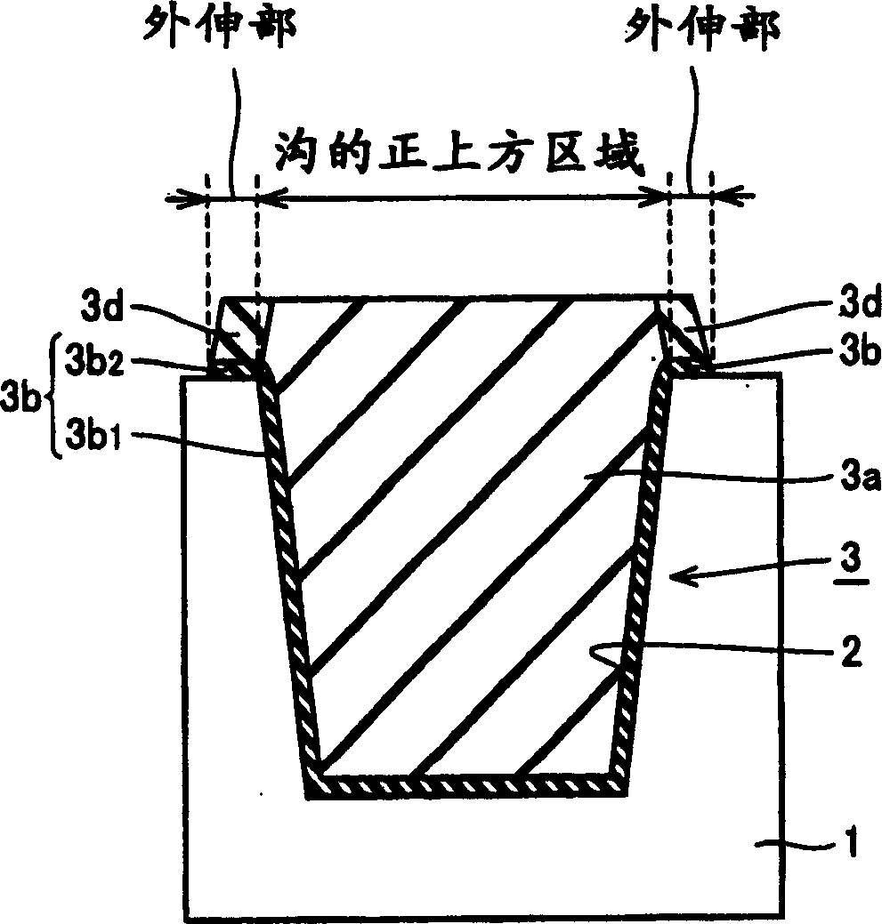
[0044] refer to figure 2 , compared with the structure of Embodiment 2, the difference of the structure of this embodiment is that the insulating layer 3b constituting the overhang of the buried insulating layer 3 2 and the insulating layer 3d are made of different materials from each other. insulating layer 3b 2 It is made of a thermal oxide film, and the insulating layer 3d is made of a silicon nitride film.

[0045] Since the insulating layer 3a is made of a silicon oxide film, the insulating layer 3a and the insulating layer 3d are made of different materials.

[0046] In addition, the structure other than that in this embodiment is substantially the same as that of the above-mentioned embodiment 2, and therefore the same components are denoted by the same reference numerals, and description thereof will be omitted.

[0047] According to this embodiment, since the insulating layer 3d is made of a silicon nitride film, the insulating layer 3b is removed by wet etching w...


PUM


Abstract

A semiconductor device with trench isolation is provided to restrain reverse narrow-channel effect and to obtain improved reliability from a gate insulating layer by forming a protrusion with a double insulating layer structure at both upper sidewalls of a burial insulating layer. A trench(2) is formed in a semiconductor substrate(1). A burial insulating layer(3) is filled in the trench. At this time, an upper surface of the burial insulating layer is higher than that of the substrate, so that both sidewalls of the burial insulating layer are partially exposed to the outside. A protrusion(3b2,3c) is formed at both exposed sidewalls of the burial insulating layer by stacking at least two insulating layers with each other.

Description

technical field [0001] The present invention relates to a semiconductor device with trench isolation, and more particularly to a semiconductor device with trench isolation for electrically isolating a semiconductor element from other semiconductor elements. Background technique [0002] In recent years, with the refinement of patterns in semiconductor devices, as an element isolation structure for electrically isolating semiconductor elements such as field effect transistors from other semiconductor elements, a structure called STI (Shallow Trench Isolation: Shallow Trench Isolation) is generally used. . Such STIs are disclosed in, for example, Japanese Patent Application Laid-Open Nos. 2002-100671, 2002-93900, and 11-67892. [0003] Such an STI is formed, for example, by the following steps. [0004] First, a thermal oxide film and a silicon nitride film are formed on a semiconductor substrate, and a photoresist pattern is formed on the silicon nitride film. Using the ph...

Claims


Application Information

Patent Timeline
Patent Type & Authority Applications(China)
IPC IPC(8): H01L21/76H01L21/762H01L21/8247H01L27/08H01L27/115H01L29/78H01L29/788H01L29/792
CPCH01L27/11521H01L27/115H01L21/76224H10B69/00H10B41/30B62M3/04
Inventor 杉原刚
Owner RENESAS TECH CORP
Why Eureka
Try Eureka