

Abstracted NAND logic in stacks
a stack and logic technology, applied in the field of nonvolatile storage technology, can solve problems such as not having an optimal density
- Summary
- Abstract
- Description
- Claims
- Application Information
AI Technical Summary
Benefits of technology
Problems solved by technology
Method used
Image

Examples
Embodiment Construction
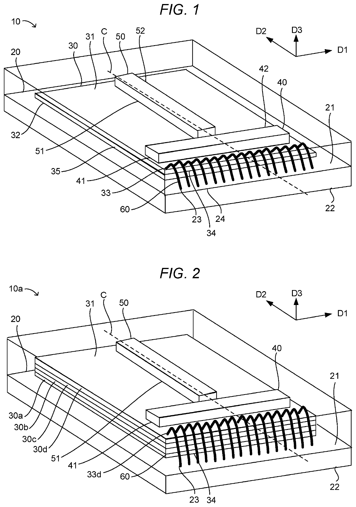
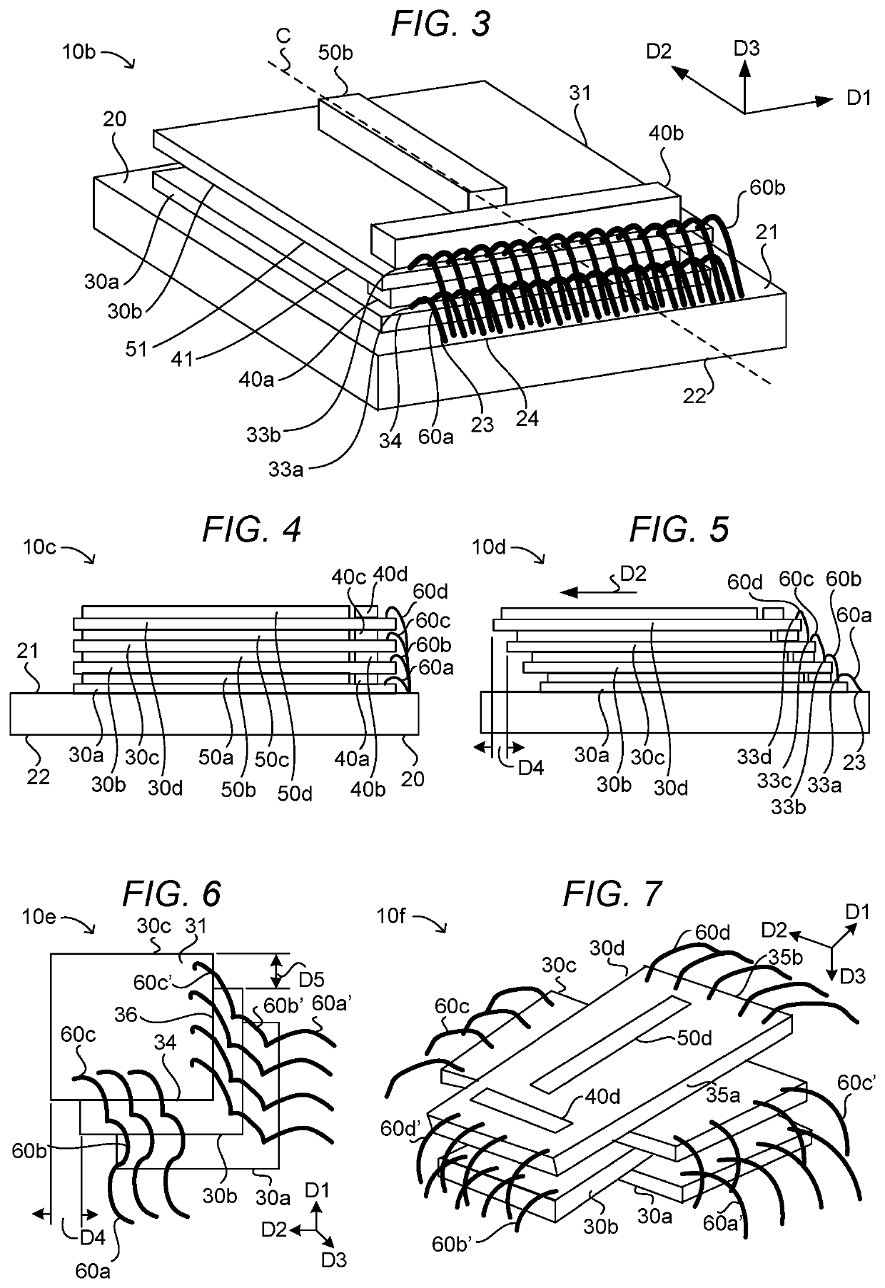
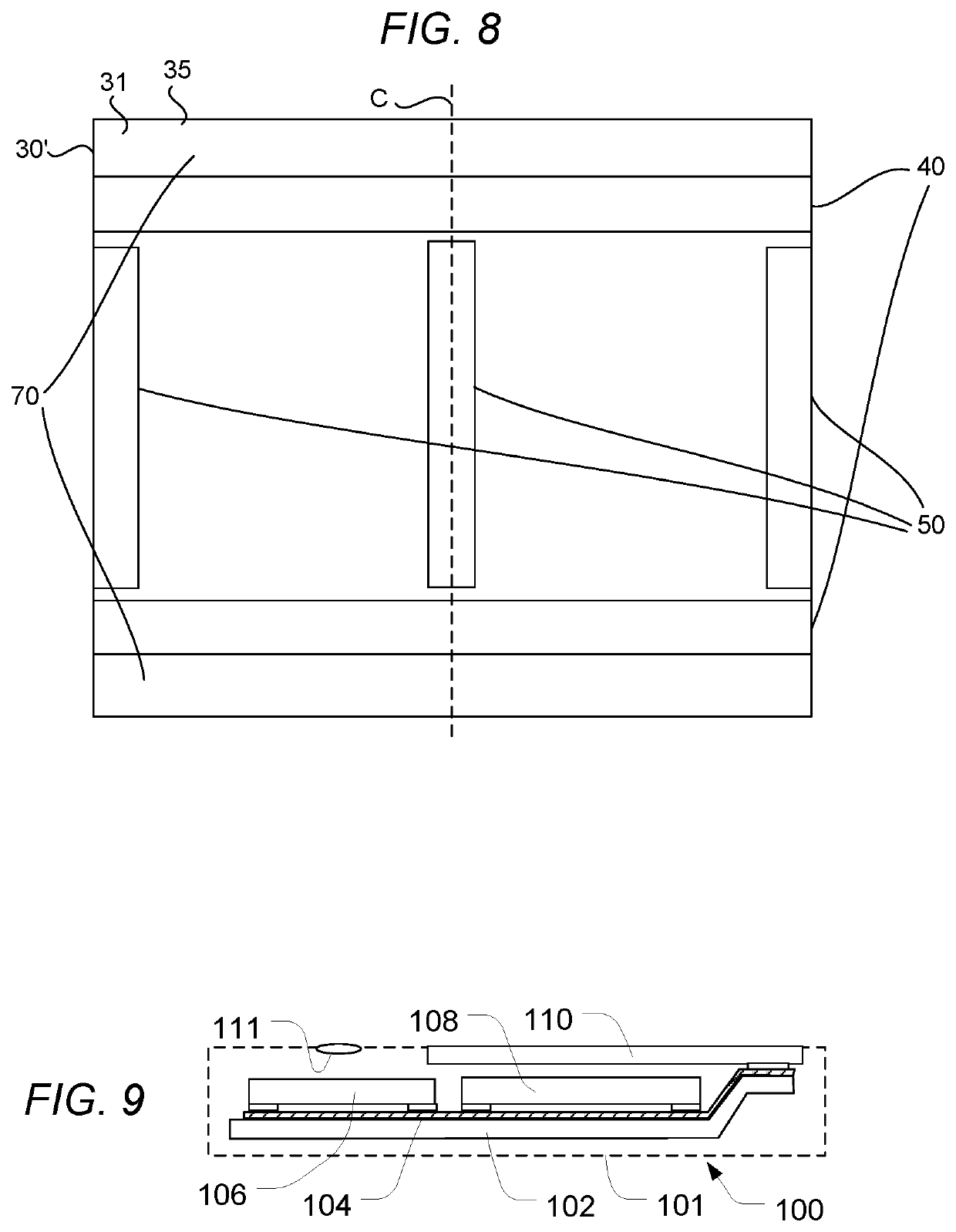
[0022]As illustrated in FIG. 1, a microelectronic package 10 may comprise a substrate 20 having first and second surfaces 21, 22, a NAND wafer 30 mounted to the first surface, a bitline driver chiplet 40, a wordline driver chiplet 50, and wire bonds 60. The substrate 20 defines first and second opposite surfaces 21, 22 that may each extend in a first direction D1 and in a second direction D2 transverse to the first direction.
[0023]As used in this disclosure with reference to the substrate 20 or another element having a planar surface, a statement that an electrically conductive element is “at” a surface of a substrate indicates that, when the substrate is not assembled with any other element, the electrically conductive element is available for contact with a theoretical point moving in a direction perpendicular to the surface of the substrate toward the surface of the substrate from outside the substrate. Thus, a terminal or other conductive element which is at a surface of a subst...
PUM
| Property | Measurement | Unit |
|---|---|---|
| thickness | aaaaa | aaaaa |
| thickness | aaaaa | aaaaa |
| electrically conductive | aaaaa | aaaaa |
Abstract
Description
Claims
Application Information