Backlight module and manufacturing method thereof, and display device

a technology of backlight module and manufacturing method, applied in semiconductor devices, identification means, instruments, etc., can solve the problems of difficulty in the difficulty of achieving the balance between light mixing and light efficiency, so as to improve the light mixing uniformity, improve the luminous efficiency of the backlight module, and increase the light-emitting angle of the led chip

Active Publication Date: 2022-04-19
WUHAN CHINA STAR OPTOELECTRONICS TECH CO LTD
View PDF8 Cites 0 Cited by
  • Summary
  • Abstract
  • Description
  • Claims
  • Application Information

AI Technical Summary

Benefits of technology

[0014]A backlight module, a manufacturing method thereof, and a display device of the present disclosure encapsulate the LED chip by a multilayer refractive index structure, significantly improving a luminous efficiency of the backlight module, increasing a light-emitting angle of the LED chip, and improving light mixing uniformity. By adopting a single-encapsulation LED chip to improve the luminous efficiency of the LED chip, less encapsulation unit materials are used and costs are reduced. The encapsulation unit adopts a multilayer encapsulation structure with a refractive index gradually decreasing outward from the LED chip and a curvature radius increasing from a side of the LED chip. Through a principle of geometrical light path, the light-emitting angle of the chip light in each dielectric film layer is gradually increased, finally achieving wide-angle light emission in an air layer, which greatly increases the light-emitting angle of the LED chip and improves the uniformity of light mixing. The manufacturing method of the present disclosure forms an encapsulation layer on the LED chip by dispensing, which is simple and conducive to mass production. At a same time, it can control refractive indexes of different encapsulation layers by changing a concentration and viscosity of an encapsulation layer material during dispensing.

Problems solved by technology

However, due to a lower light efficiency of the large-angle chips (usually 20% to 40% lower brightness than small-angle chips of a same size), it is difficult to achieve a balance between light mixing and light efficiency.
Therefore, how to achieve the balance between light mixing and light efficiency has become a difficulty in current technological development.

Method used


Image

  • Backlight module and manufacturing method thereof, and display device
  • Backlight module and manufacturing method thereof, and display device

Examples


embodiment 1

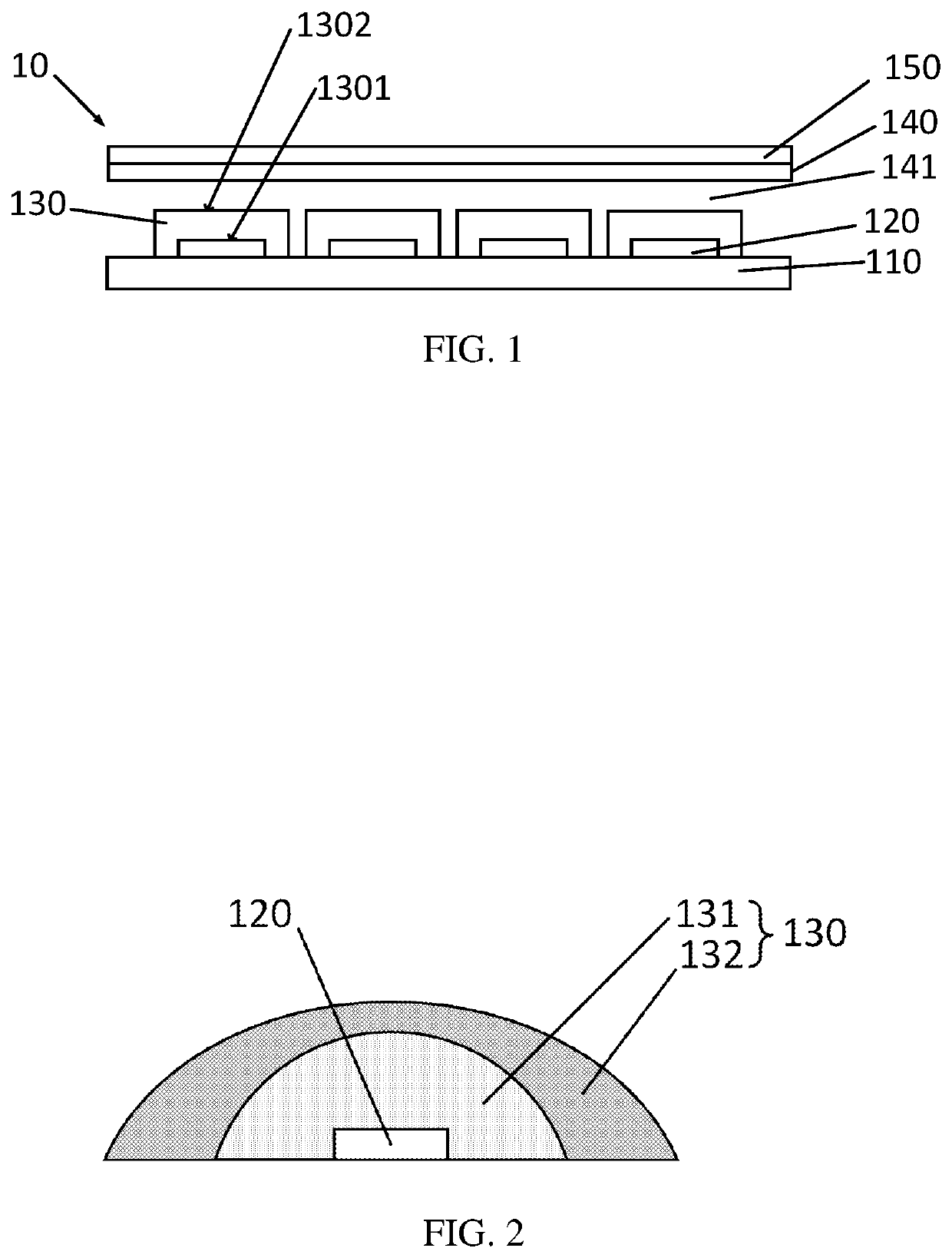
[0022]As shown in FIG. 1, in this embodiment, a backlight module 10 of the present disclosure includes a substrate 110, a plurality of LED chips 120, a plurality of first encapsulation units 130, a diffusion layer 140, and a light enhancement layer 150.

[0023]The substrate 110 is an FPC flexible board or a PCB / BT hardboard, and the plurality of the LED chips 120 are distributed on the substrate 110. The plurality of LED chips 120 are uniformly bonded to the substrate 110 by solder, and by replacing a backlight with separate light sources of the plurality of LED chips 120, local adjustment of an image can be achieved, thus increasing a contrast.

[0024]To increase a light-emitting angle and a light-emitting efficiency of the LED chips 120 of the backlight module 10 of the present disclosure, in this embodiment, one of the plurality of first encapsulation units 130 is used to encapsulate the LED chips 120 individually, and adjacent first encapsulation units 130 are not in contact with ea...

embodiment 2

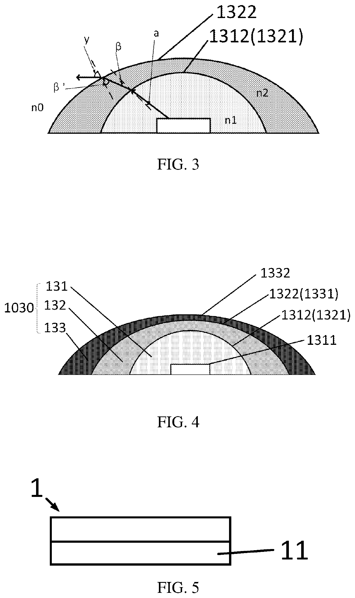
[0032]As shown in FIG. 4, a structure of a backlight module 11 in this embodiment is similar to the backlight module 10 of embodiment 1. The difference is that a second encapsulation unit 1030 in this embodiment further includes a third encapsulation layer 133. The third encapsulation layer 133 includes a third light-incident surface 1331 and a third light-exiting surface 1332. The third light-incident surface 1331 and the second light-exiting surface 1322 of the second encapsulation layer 132 are bonded together. A shape of the third light-incident surface 1331 is a curved inner concave surface, and is adapted to the second light-exiting surface 1322 to ensure that light enters the third light-incident surface 1331 directly after exiting from the second light-exiting surface 1322. The third light-exiting surface 1332 is an arc-shaped convex surface, and a radius of curvature thereof is greater than a radius of curvature of the second light-exiting surface 1322, thereby achieving th...


PUM

PropertyMeasurementUnit
refractive indexaaaaaaaaaa
radian of curvatureaaaaaaaaaa

Abstract

The present disclosure provides a backlight module, a manufacturing method thereof, and a display device. The backlight module including a substrate, a plurality of LED chips disposed on the substrate, a plurality of encapsulation units encapsulating the LED chips in a one-to-one correspondence; each of the encapsulation units includes at least two encapsulation layers, an innermost one of the encapsulation layers completely covers the LED chip, and a refractive index of an encapsulation layer far from the LED chip is less than a refractive index of an encapsulation layer near the LED chip.

Description

FIELD OF INVENTION[0001]The present disclosure relates to the field of display technologies, and more particularly, to a display module and a manufacturing method thereof, and a display device.BACKGROUND OF INVENTION[0002]Mini-LEDs are currently hot spots on the market, and have a type of direct-type light-emitting backlight module. Compared with traditional direct-type backlight modules, the mini-LEDs have many advantages, such as being ultra-thin, flexible and bendable, and having an ability to achieve narrow bezels, local dimming (local backlight adjustment), etc. Local backlight adjustment uses a backlight consisting of hundreds of LEDs instead of cold cathode fluorescent lamp (CCFL), and can adjust the backlight LEDs according to a brightness of an image. Therefore, highlights in a display screen image can reach a maximum value, while brightness of dark portions can be maximumly decreased and even turned off to increase a contrast, which reduces backlight power consumption.[000...

Claims


Application Information

Patent Timeline
Patent Type & Authority Patents(United States)
IPC IPC(8): H01L25/075H01L33/54H01L33/56H01L33/58
CPCH01L25/0753H01L33/54H01L33/56H01L33/58H01L2933/005H01L33/52G09F9/30G02F1/133603G02F1/133611G02F1/133606H01L2933/0058G02F1/133607
Inventor YANG, YONG
Owner WUHAN CHINA STAR OPTOELECTRONICS TECH CO LTD
Why Eureka
Try Eureka