Three-dimensional semiconductor memory device

a semiconductor memory and three-dimensional technology, applied in semiconductor devices, semiconductor/solid-state device details, electrical equipment, etc., can solve the problems of increasing pattern fineness, requiring very expensive equipment, and practical limitation of pattern fineness, so as to reduce process failure

Active Publication Date: 2022-08-02
SAMSUNG ELECTRONICS CO LTD
View PDF13 Cites 3 Cited by
  • Summary
  • Abstract
  • Description
  • Claims
  • Application Information

AI Technical Summary

Benefits of technology

[0004]An exemplary embodiment of the present inventive concepts provides a three-dimensional semiconductor memory device with an increased integration density.
[0005]An exemplary embodiment of the present inventive concepts provides a method of reducing a process failure in a process of fabricating a three-dimensional semiconductor memory device.

Problems solved by technology

However, an increase in the pattern fineness requires very expensive equipment and there is a practical limitation on the pattern fineness.

Method used


Image

  • Three-dimensional semiconductor memory device
  • Three-dimensional semiconductor memory device
  • Three-dimensional semiconductor memory device

Examples


Embodiment Construction

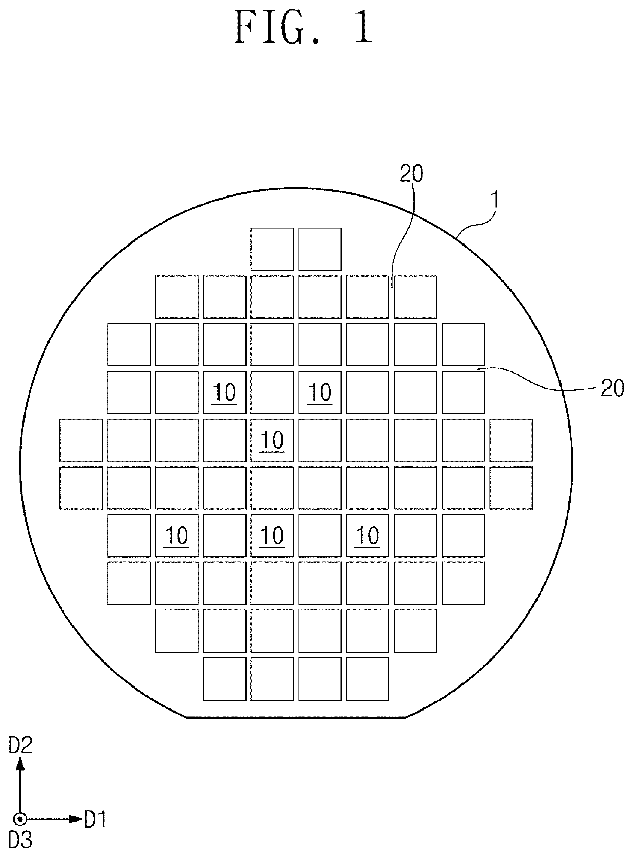
[0026]FIG. 1 is a top plan view illustrating a substrate, on which three-dimensional semiconductor memory devices according to an exemplary embodiment of the present inventive concepts are integrated.

[0027]Referring to FIG. 1, a semiconductor substrate 1 (e.g., a wafer, etc.) may include chip regions 10 which include semiconductor chips formed thereon, and a scribe line region 20, located between the chip regions 10. In an exemplary embodiment, the semiconductor substrate 1 may include a plurality of discrete chip regions that are two-dimensionally arranged in two different directions (e.g., a first direction D1 and a second direction D2). Each of the chip regions 10 may be surrounded by the scribe line region 20. In other words, the scribe line region 20 may be disposed between each adjacent pair of the chip regions 10, which are adjacent to each other in the first and / or second directions D1 and D2. While the chip regions 10 are shown in the exemplary embodiment of FIG. 1 as compr...


PUM


Abstract

A semiconductor memory device includes horizontal patterns disposed on a peripheral circuit structure and spaced apart from each other in a first direction. Memory structures are disposed on the horizontal patterns. The memory structures include source structures and electrode structures. A division structure is disposed between adjacent horizontal patterns in the first direction and is configured to separate the source structures of adjacent memory structures from each other. An etch stop pattern is disposed between the horizontal patterns at a level lower than a level of the source structures. The etch stop pattern is connected to a lower portion of the division structure.

Description

CROSS-REFERENCE TO RELATED APPLICATION[0001]This application claims priority under 35 U.S.C. § 119 to Korean Patent Application No. 10-2019-0094346, filed on Aug. 2, 2019 in the Korean Intellectual Property Office, the disclosure of which is incorporated by reference in its entirety herein.TECHNICAL FIELD[0002]The present inventive concepts relate to a three-dimensional semiconductor memory device and a method of fabricating the same, and in particular, to a highly-integrated three-dimensional semiconductor memory device and a method of fabricating the same.DISCUSSION OF RELATED ART[0003]Consumer demand for electronic devices that provide a superior performance and are relatively inexpensive has resulted in the need for higher integration of semiconductor devices. In the case of two-dimensional or planar semiconductor devices, since their integration is mainly determined by the area occupied by a unit memory cell, integration is greatly influenced by the level of a fine pattern form...

Claims


Application Information

Patent Timeline
Patent Type & Authority Patents(United States)
IPC IPC(8): H01L27/11582H01L27/11519H01L27/11524H01L27/11529H01L23/522H01L27/11565H01L27/1157H01L27/11573H01L27/11556
CPCH01L27/11582H01L23/5226H01L27/1157H01L27/11519H01L27/11524H01L27/11529H01L27/11556H01L27/11565H01L27/11573H10B41/10H10B41/40H10B43/10H10B41/27H10B43/40H10B43/27H01L29/792H10B43/35H10B41/35H10B41/41
Inventor SIM, JAERYONGAHN, JONGSEONHAN, JEEHOON
Owner SAMSUNG ELECTRONICS CO LTD
Why Eureka
Try Eureka