

Display apparatus and method of fabricating the same
- Summary
- Abstract
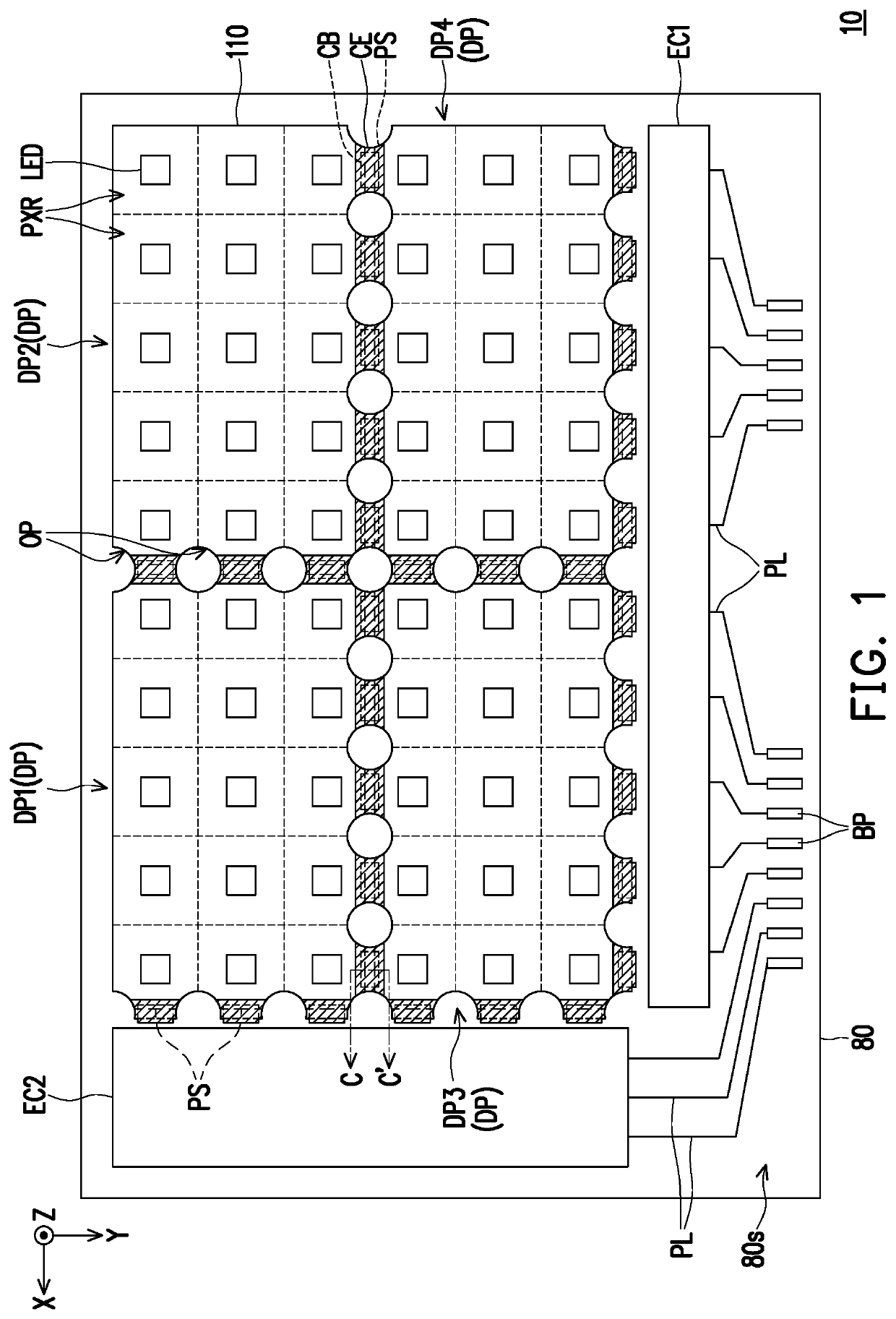
- Description
- Claims
- Application Information
AI Technical Summary
Benefits of technology
Problems solved by technology
Method used
Image

Examples
Embodiment Construction
[0035]“About”, “similar”, “essentially”, or “substantially” used in the present specification include the value and the average value within an acceptable deviation range of a specific value confirmed by those having ordinary skill in the art, and the concerned measurement and a specific quantity (i.e., limitations of the measuring system) of measurement-related errors are taken into consideration. For instance, “about” may represent within one or a plurality of standard deviations of the value, or, for instance, within ±30%, ±20%, ±15%, ±10%, or ±5%. Moreover, “about”, “similar”, “essentially”, or “substantially” used in the present specification may include a more acceptable deviation range or standard deviation according to measurement properties, cutting properties, or other properties, and one standard deviation does not need to apply to all of the properties.
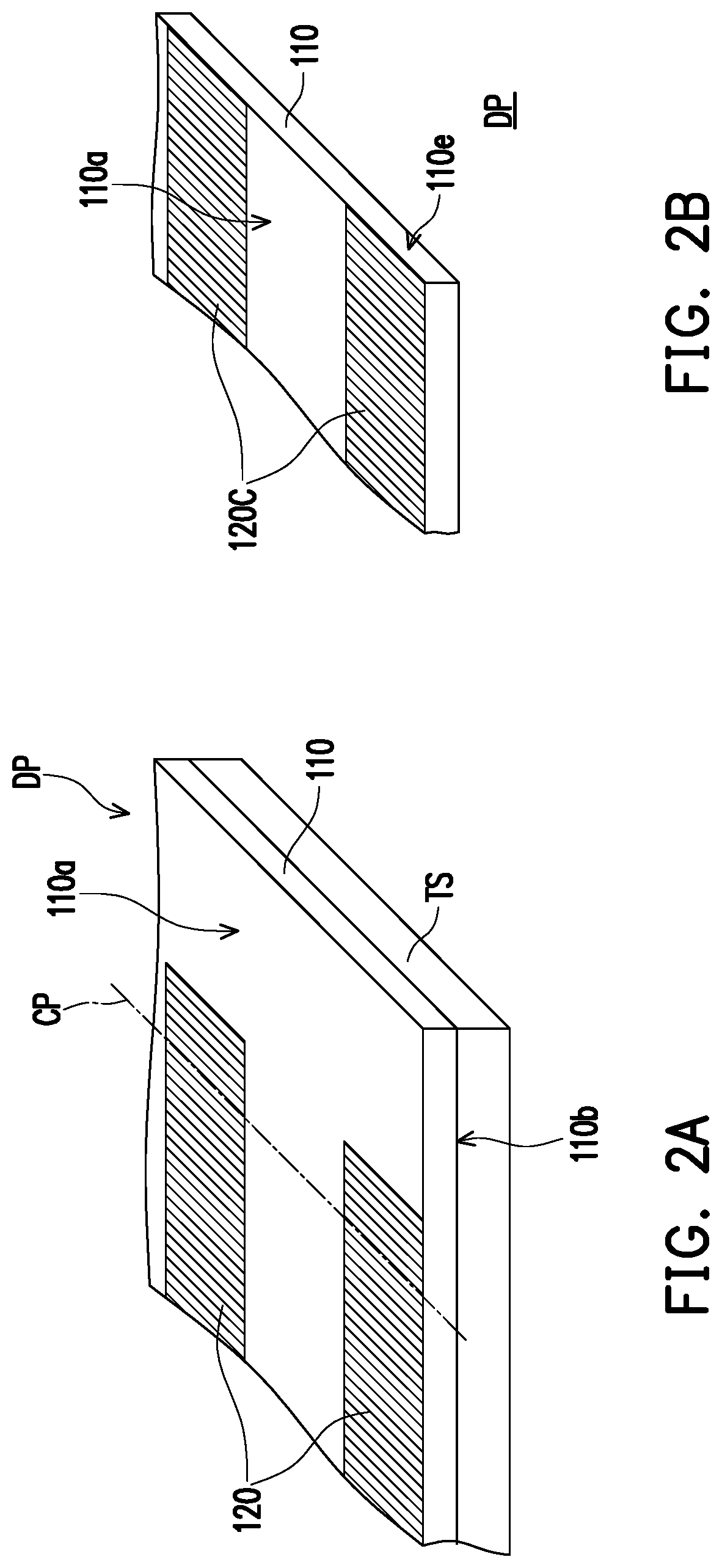
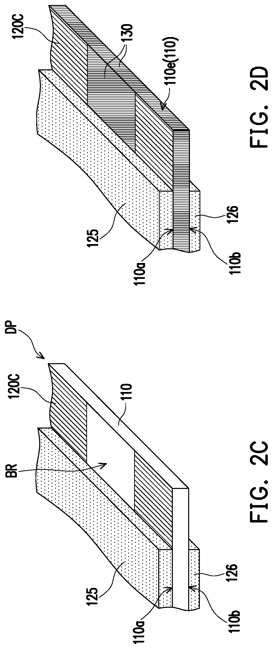
[0036]In the figures, for clarity, the thicknesses of, for instance, layers, films, panels, and regions are enlarged. It...
PUM
| Property | Measurement | Unit |
|---|---|---|
| conductive | aaaaa | aaaaa |
| width | aaaaa | aaaaa |
| organic | aaaaa | aaaaa |
Abstract
Description
Claims
Application Information