
Display apparatus and method of fabricating the same

a technology of display apparatus and assembly method, which is applied in the direction of identification means, instruments, semiconductor devices, etc., to achieve the effect of ensuring the electrical independence increasing the bonding area of the pad structure, and increasing the bonding (or tiling) yield of the display panel

Active Publication Date: 2021-07-15
AU OPTRONICS CORP
View PDF0 Cites 5 Cited by
  • Summary
  • Abstract
  • Description
  • Claims
  • Application Information

AI Technical Summary

Benefits of technology

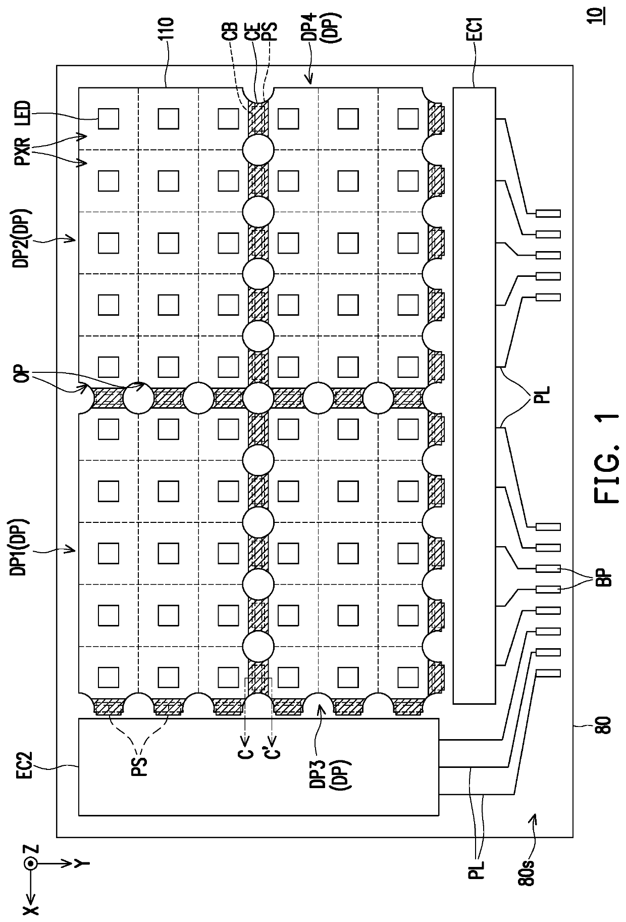
The invention is about a display screen that has better electrical properties, can be made bigger and have higher resolution. The invention also describes a method for making the screen that increases the yield of the tiling process and makes the screen easier to design. The invention uses openings between the pads on the screen to make them electrically independent, which ensures better stability and increased yield. Overall, the invention improves the performance and reliability of the display screen.

Problems solved by technology

However, with the increase in the resolution and driving frequency of light-emitting diode panels, the stability of signal transmission, the increase in driving current, and the electrical properties of driving circuits have become important issues that related manufacturers must address in the development process.

Method used


Image

  • Display apparatus and method of fabricating the same
  • Display apparatus and method of fabricating the same
  • Display apparatus and method of fabricating the same

Examples


Embodiment Construction

[0035]“About”, “similar”, “essentially”, or “substantially” used in the present specification include the value and the average value within an acceptable deviation range of a specific value confirmed by those having ordinary skill in the art, and the concerned measurement and a specific quantity (i.e., limitations of the measuring system) of measurement-related errors are taken into consideration. For instance, “about” may represent within one or a plurality of standard deviations of the value, or, for instance, within ±30%, ±20%, ±15%, ±10%, or ±5%. Moreover, “about”, “similar”, “essentially”, or “substantially” used in the present specification may include a more acceptable deviation range or standard deviation according to measurement properties, cutting properties, or other properties, and one standard deviation does not need to apply to all of the properties.

[0036]In the figures, for clarity, the thicknesses of, for instance, layers, films, panels, and regions are enlarged. It...


PUM

PropertyMeasurementUnit
conductiveaaaaaaaaaa
widthaaaaaaaaaa
organicaaaaaaaaaa

Abstract

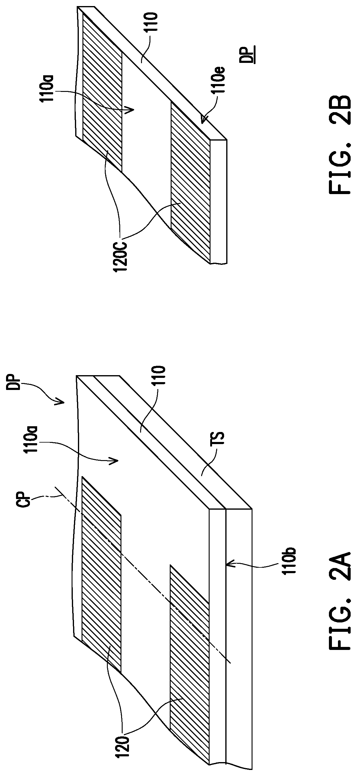
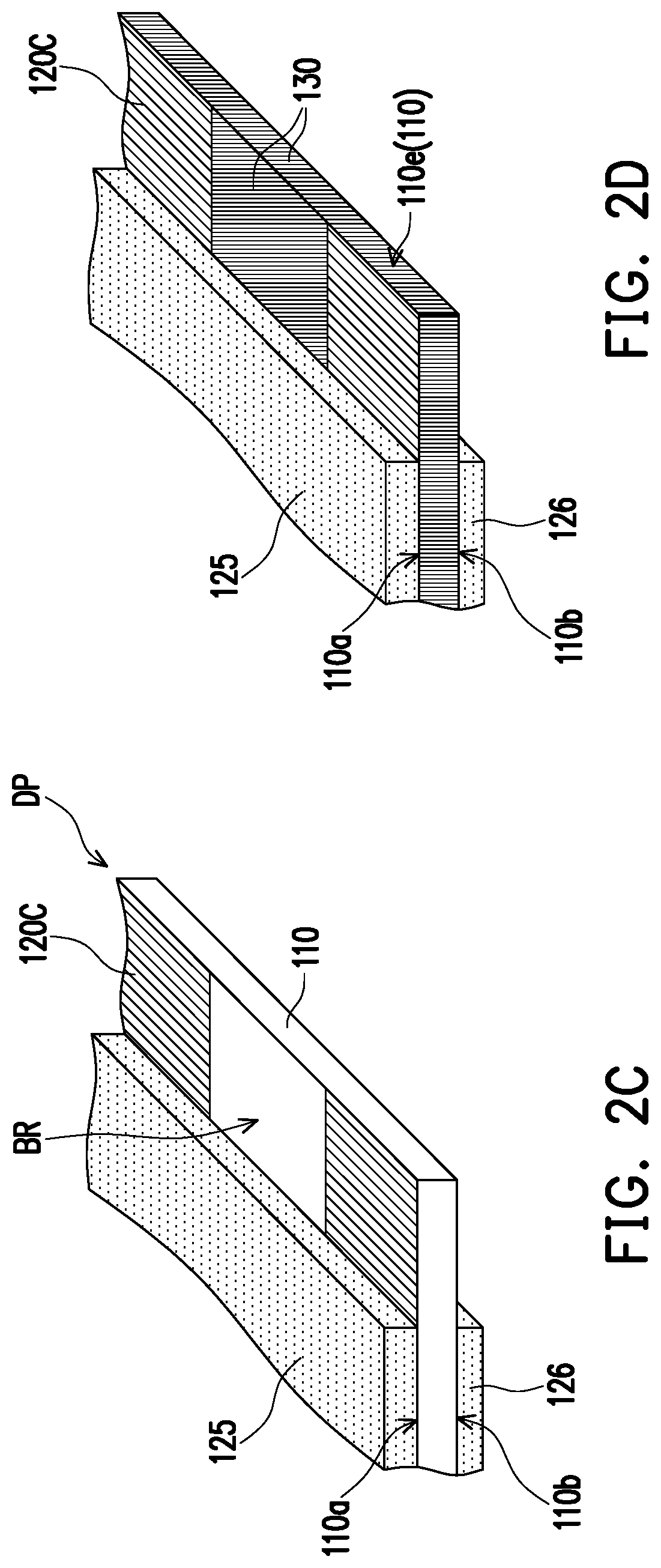
A display apparatus including at least one display panel is provided. The display panel includes a substrate, pad structures, and openings. The substrate has a first and second surface opposite to each other. The pad structures are disposed on the first surface of the substrate. Each pad structure has a connection pad, a conductive pattern layer, and an auxiliary conductive layer electrically connected to each other. The auxiliary conductive layer is overlapped with the conductive pattern layer and the connection pad along a normal direction of the first surface. The openings are disposed on the substrate and penetrate the first and second surfaces of the substrate. The openings and the pad structures are alternately arranged. The substrate also has a third surface defining each opening and connected to the first and second surfaces. The third surface is not conductive. A method of fabricating the display apparatus is also provided.

Description

CROSS-REFERENCE TO RELATED APPLICATION[0001]This application claims the priority benefits of U.S. provisional application Ser. No. 62 / 960,846, filed on Jan. 14, 2020, and Taiwan application serial no. 109115866, filed on May 13, 2020. The entirety of each of the above-mentioned patent applications is hereby incorporated by reference herein and made a part of this specification.BACKGROUND OF THE INVENTIONField of the Invention[0002]The invention relates to a display apparatus, and more particularly to a display apparatus having a light-emitting element.Description of Related Art[0003]With the gradual diversification of the applications of the display apparatus, the use of large display boards for displaying public information or advertisements in major exhibition halls or department stores is becoming increasingly popular. In order to reduce the cost of installation and maintenance of large display boards, tiled displays formed by tiling a plurality of display panels have become one ...

Claims


Application Information

Patent Timeline
Patent Type & Authority Applications(United States)
IPC IPC(8): H01L27/15H01L33/62H01L33/00
CPCH01L27/156H01L2933/0066H01L33/0095H01L33/62G09F9/30G09F9/302G09F9/3026H01L25/0753G02F1/13336G02F1/13458
Inventor XI, PENG-BOCHENG, CHUN-CHENG
Owner AU OPTRONICS CORP
Learn More