
Electronic device having housing

a technology of electronic devices and housings, which is applied in the direction of casings/cabinets/drawer details, instruments, and casings with display/control units, etc., can solve the problems of reducing the strength of wear resistance (including the coating layer), affecting the performance of the device, so as to reduce the wear resistance deterioration and ensure the effect of productivity

Active Publication Date: 2022-09-27
SAMSUNG ELECTRONICS CO LTD
View PDF17 Cites 0 Cited by
  • Summary
  • Abstract
  • Description
  • Claims
  • Application Information

AI Technical Summary

Benefits of technology

The patent describes an electronic device with a film structure that can create a haze feeling, which increases productivity and reduces wear and tear. The device has a roughness structure with an uneven shape that can achieve various haze feelings. This patent aims to improve the overall quality of electronic devices.

Problems solved by technology

However, when the haze feeling is implemented by constructing a high roughness in at least part of the housing of the electronic device, there may be a throughput deterioration such as a stain or the like occurring in processes.
An increase in a surface roughness may lead to a decrease in strength of a wear resistance (including a coating layer), and there may be a difference in the roughness, compared to a degree of roughness implemented through sanding or etching.
For another example, when the haze feeling is applied to a surface of an external glass plate directly through sanding or etching, it may be vulnerable to impact strength

Method used


Image

  • Electronic device having housing
  • Electronic device having housing
  • Electronic device having housing

Examples


Embodiment Construction

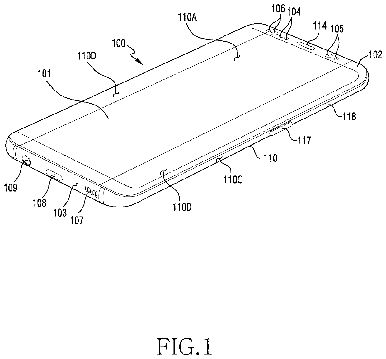
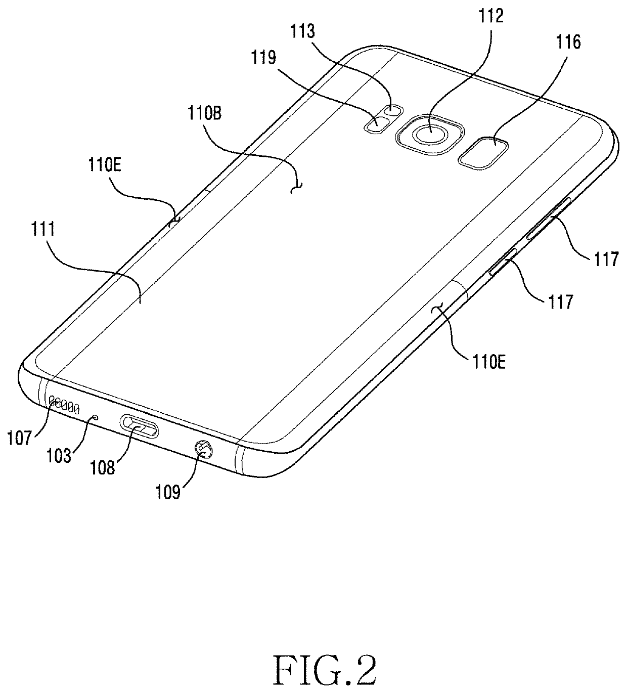
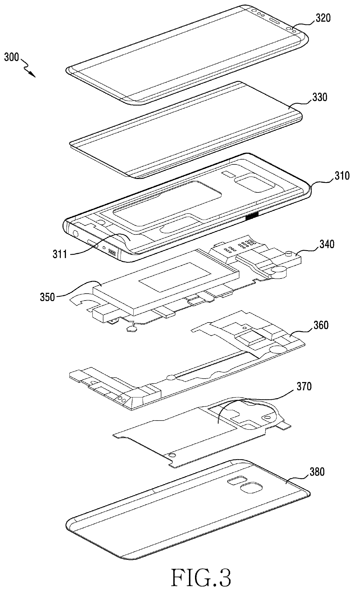
[0028]FIGS. 1 through 12, discussed below, and the various embodiments used to describe the principles of the present disclosure in this patent document are by way of illustration only and should not be construed in any way to limit the scope of the disclosure. Those skilled in the art will understand that the principles of the present disclosure may be implemented in any suitably arranged system or device.

[0029]Hereinafter, various embodiments of the disclosure are described with reference to the accompanying drawings. It should be appreciated that various embodiments of the disclosure and the terms used therein are not intended to limit the technological features set forth herein to particular embodiments and include various changes, equivalents, or replacements for a corresponding embodiment. With regard to the description of the drawings, similar reference numerals may be used to refer to similar or related elements.

[0030]An electronic device according to various embodiments of ...


PUM

PropertyMeasurementUnit
diameteraaaaaaaaaa
diameteraaaaaaaaaa
roughnessaaaaaaaaaa

Abstract

An electronic device includes a housing including a first plate, a second plate facing away from the first plate, and a lateral member surrounding a space between the first plate and the second plate; a display visible through at least part of the first plate; and a glass construction constructing at least part of the second plate. The glass construction includes a glass plate including a first face outwardly facing the housing and a second face facing away from the first face, an inorganic layer including a first roughness and constructed on the first face, a first polymer layer disposed between the first plate and the second face, an Optically Clear Adhesive (OCA) layer disposed between the second face and the first polymer layer, and a second polymer layer disposed between the first plate and the first polymer layer and including a third face and a fourth face.

Description

CROSS-REFERENCE TO RELATED APPLICATION[0001]This application is based on and claims priority under 35 U.S.C. 119 to Korean Patent Application No. 10-2019-0001133 filed on Jan. 4, 2019 in the Korean Intellectual Property Office, the disclosure of which is herein incorporated by reference in its entirety.BACKGROUND1. Field[0002]Various embodiments of the disclosure relate to a housing of an electronic device.2. Description of Related Art[0003]At least part of a housing of an electronic device may be constructed of synthetic resin or a glass material.[0004]At least part of the housing may implement a visual haze feeling due to a scattering effect of light by applying and curing a coating liquid to an outer face through a wet spray to constitute a roughness, e.g., a fine uneven structure, on an outer surface.[0005]However, when the haze feeling is implemented by constructing a high roughness in at least part of the housing of the electronic device, there may be a throughput deterioratio...

Claims


Application Information

Patent Timeline
Patent Type & Authority Patents(United States)
IPC IPC(8): G02B5/04G02B27/01
CPCG02B5/045G02B27/01G06F1/1637B32B27/02C03C17/3405H05K5/03H05K5/0017C03C17/3649C03C17/3642
Inventor HAN, SOONHOKIM, YOOJINLEE, HYUNGGONCHOI, JONGCHUL
Owner SAMSUNG ELECTRONICS CO LTD
Learn More