Red light emitting diode and manufacturing method thereof

a technology manufacturing methods, which is applied in the direction of basic electric elements, electrical equipment, semiconductor devices, etc., can solve the problems of limiting the applicability of red light emitting diodes and the effective reduction of the volume of light emitting diodes

Active Publication Date: 2022-11-22
GENESIS PHOTONICS
View PDF26 Cites 0 Cited by
  • Summary
  • Abstract
  • Description
  • Claims
  • Application Information

AI Technical Summary

Benefits of technology

[0030]To sum up, since the red light emitting diode in the embodiments of the disclosure is provided in a form of a flip-chip light emitting diode, the red light emitting diode may be electrically connected to an external substrate (e.g., an array substrate of a display) in a flip-chip manner through the two electrode pads by an eutectic process. In this way, arrangement of a wire-bonding region may be omitted, so that a volume of a light emitting diode device (e.g., a light emitting diode display) may be effectively reduced, and favorable applicability is thereby provided. Besides, since the red light emitting diode is a flip-chip light emitting diode, heat dissipation may be performed through the internal first and second electrodes and the first and the second electrode pads to dissipate heat to the outside, and that heat dissipation efficiency is improved. In addition, the manufacturing method of manufacturing the red light emitting diode is also provided in the disclosure.

Problems solved by technology

Arrangement of the wire-bonding region prevents the volume of the light emitting diode display from being effectively reduced, and applicability of the red light emitting diode is thereby considerably limited.

Method used


Image

  • Red light emitting diode and manufacturing method thereof
  • Red light emitting diode and manufacturing method thereof
  • Red light emitting diode and manufacturing method thereof

Examples


Embodiment Construction

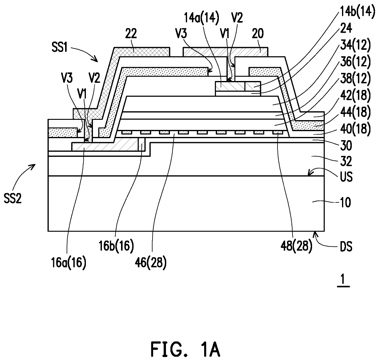
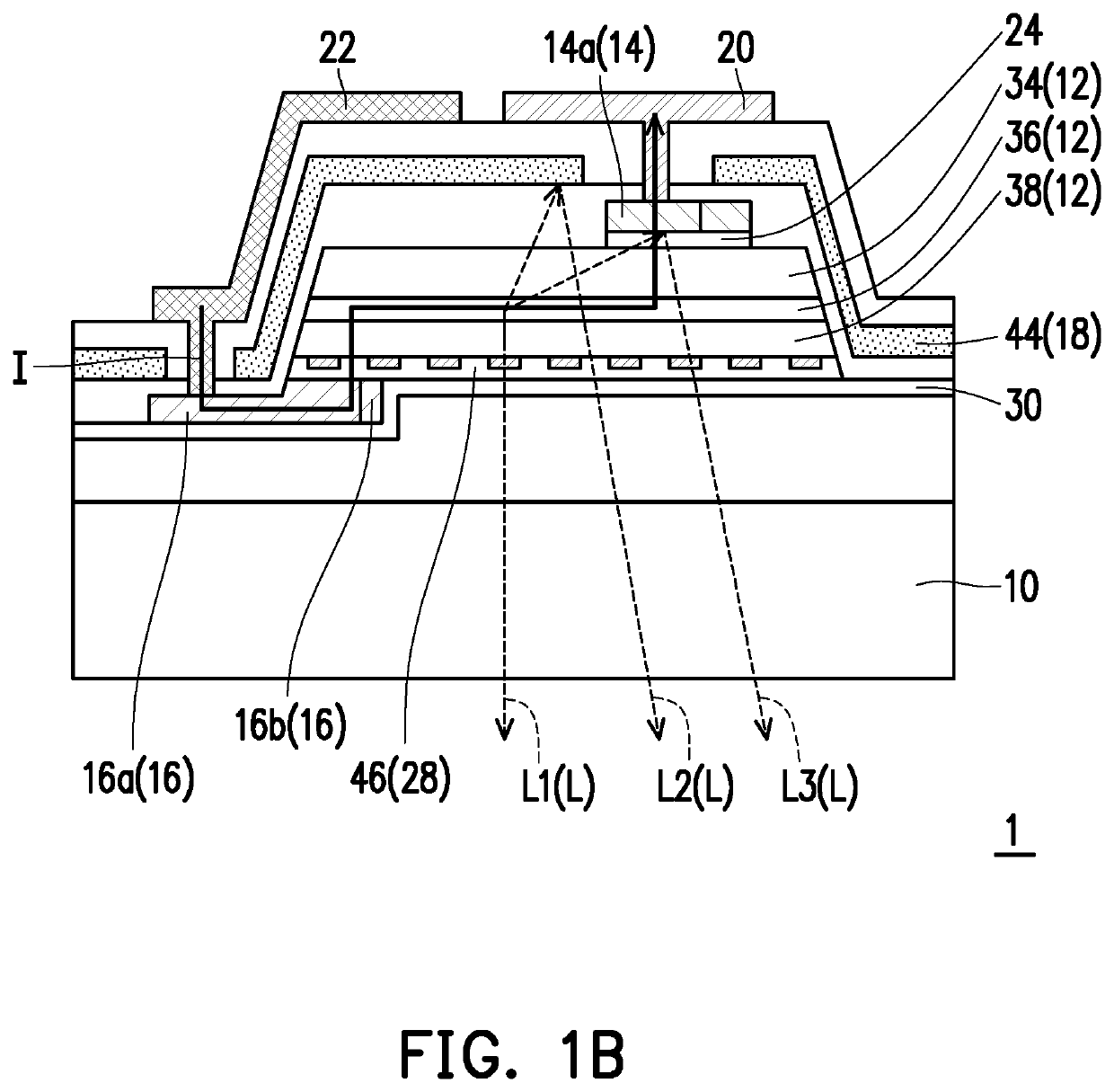
[0041]FIG. 1A is a schematic cross-sectional view of a red light emitting diode according to an embodiment of the disclosure. FIG. 1B is schematic diagram of a current path and an optical effect of the red light emitting diode in FIG. 1A.

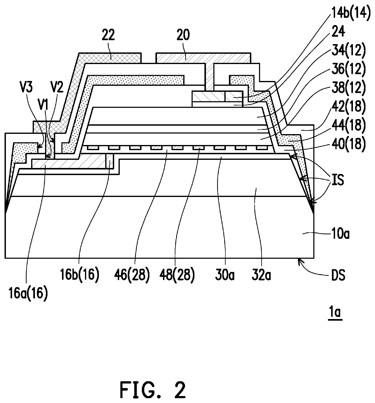
[0042]With reference to FIG. 1A, a red light emitting diode 1 includes a substrate 10, an epitaxial stacked layer 12, a first electrode 14, a second electrode 16, a reflective stacked layer 18, a first electrode pad 20, a second electrode pad 22, a semiconductor layer 24, a conductive structure layer 28, a lower insulating layer 30, and a bonding layer 32. The foregoing devices are described in detail in the following paragraphs.

[0043]The substrate 10 is mainly configured carry the abovementioned elements and may also be called as a carrying substrate. The substrate 10 has an upper and a lower surfaces US and DS opposite to each other, and a material thereof may include a sapphire substrate, a glass substrate, or a transparent substrate.

[0044]The ep...


PUM

PropertyMeasurementUnit
light emitting wavelengthaaaaaaaaaa
wavelengthaaaaaaaaaa
semiconductoraaaaaaaaaa

Abstract

A red light emitting diode including an epitaxial stacked layer, a first and a second electrodes and a first and a second electrode pads is provided. The epitaxial stacked layer includes a first-type and a second-type semiconductor layers and a light emitting layer. A main light emitting wavelength of the light emitting layer falls in a red light range. The epitaxial stacked layer has a first side adjacent to the first semiconductor layer and a second side adjacent to the second semiconductor layer. The first and the second electrodes are respectively electrically connected to the first-type and the second-type semiconductor layers, and respectively located to the first and the second sides. The first and a second electrode pads are respectively disposed on the first and the second electrodes and respectively electrically connected to the first and the second electrodes. The first and the second electrode pads are located at the first side of the epitaxial stacked layer. Furthermore, a manufacturing method of the red light emitting diode is also provided.

Description

CROSS-REFERENCE TO RELATED APPLICATION[0001]This application claims the priority benefit of U.S. provisional application Ser. No. 62 / 822,070, filed on Mar. 22, 2019. The entirety of the above-mentioned patent application is hereby incorporated by reference herein and made a part of this specification.BACKGROUNDTechnical Field[0002]The disclosure relates to a light emitting diode and a manufacturing method thereof, and in particular, to a red light emitting diode and a manufacturing method thereof.Description of Related Art[0003]Light emitting diodes are widely applied to different fields thanks to their favorable photoelectric properties. Moreover, light emitting diodes are regarded as the mainstream of the next-generation display technology in recent years owing to low costs and good display effects provided by the light emitting diodes.[0004]Generally, light emitting diodes of red light, blue light, green light, etc. are disposed in each pixel in a light emitting diode display mos...

Claims


Application Information

Patent Timeline
Patent Type & Authority Patents(United States)
IPC IPC(8): H01L33/38H01L33/62H01L33/42H01L33/00H01L33/10
CPCH01L33/382H01L33/0095H01L33/10H01L33/42H01L33/62H01L2933/0016H01L2933/0066H01L33/48H01L33/647H01L33/005H01L33/385H01L33/387H01L33/46
Inventor CHUANG, TUNG-LINHUANG, YI-RUKUO, YU-CHENSHEN, CHIH-MINGHUANG, TSUNG-SYUNHUANG, JING-EN
Owner GENESIS PHOTONICS
Why Eureka
Try Eureka