Inductively coupled plasma CVD

a plasma cvd and inductive coupling technology, applied in the field of inductive coupling plasma cvd, can solve the problems of high cost, complex ecr and helicon sources which rely on magnetic fields, and unsuitable techniques for gap widths below 0.5 microns,

Inactive Publication Date: 2001-09-06
SHUFFLEBOTHAM PAUL KEVIN +5
View PDF44 Cites 51 Cited by
  • Summary
  • Abstract
  • Description
  • Claims
  • Application Information

AI Technical Summary

Problems solved by technology

That single step process replaced sequential gap-filling and planarization steps wherein CVD SiO.sub.2 was subjected to plasma etch-back steps, such technique being unsuitable for gap widths below 0.5 microns and aspect ratios (gap height:width) above 1.5:1.
Prior art apparatuses suffer from several serious disadvantages with respect to IMD applications.
ECR and helicon sources which rely on magnetic fields are complex and expensive.
Moreover, magnetic fields have been implicated to cause damage to semiconductor devices on the wafer.
ECR, helicon and helical resonator sources also generate plasmas remotely from the wafer, making it very difficult to produce uniform and high quality films at the same time and also difficult to perform in-situ plasma cleans necessary to keep particulates under control without additional equipment.
Furthermore, ECR, helicon and helical resonator, and domed inductively-coupled plasma systems require large, complex dielectric vacuum vessels.
As a corollary scale-up is difficult and in-situ plasma cleaning is time consuming.
In the absence of an RF bias, the film quality and gap-filling performance tend to be poor due to a jagged appearance of the sidewall film suggesting that it is very porous and heavy deposits forming above metal lines shadow the trench bottoms from deposition and eventually pinch-off the gap, leaving a void.
This results in choked, sonic flow at the outlets of the injectors.

Method used


Image

  • Inductively coupled plasma CVD
  • Inductively coupled plasma CVD
  • Inductively coupled plasma CVD

Examples


example ii

[0068] (Gap-fill and Capping Processes)

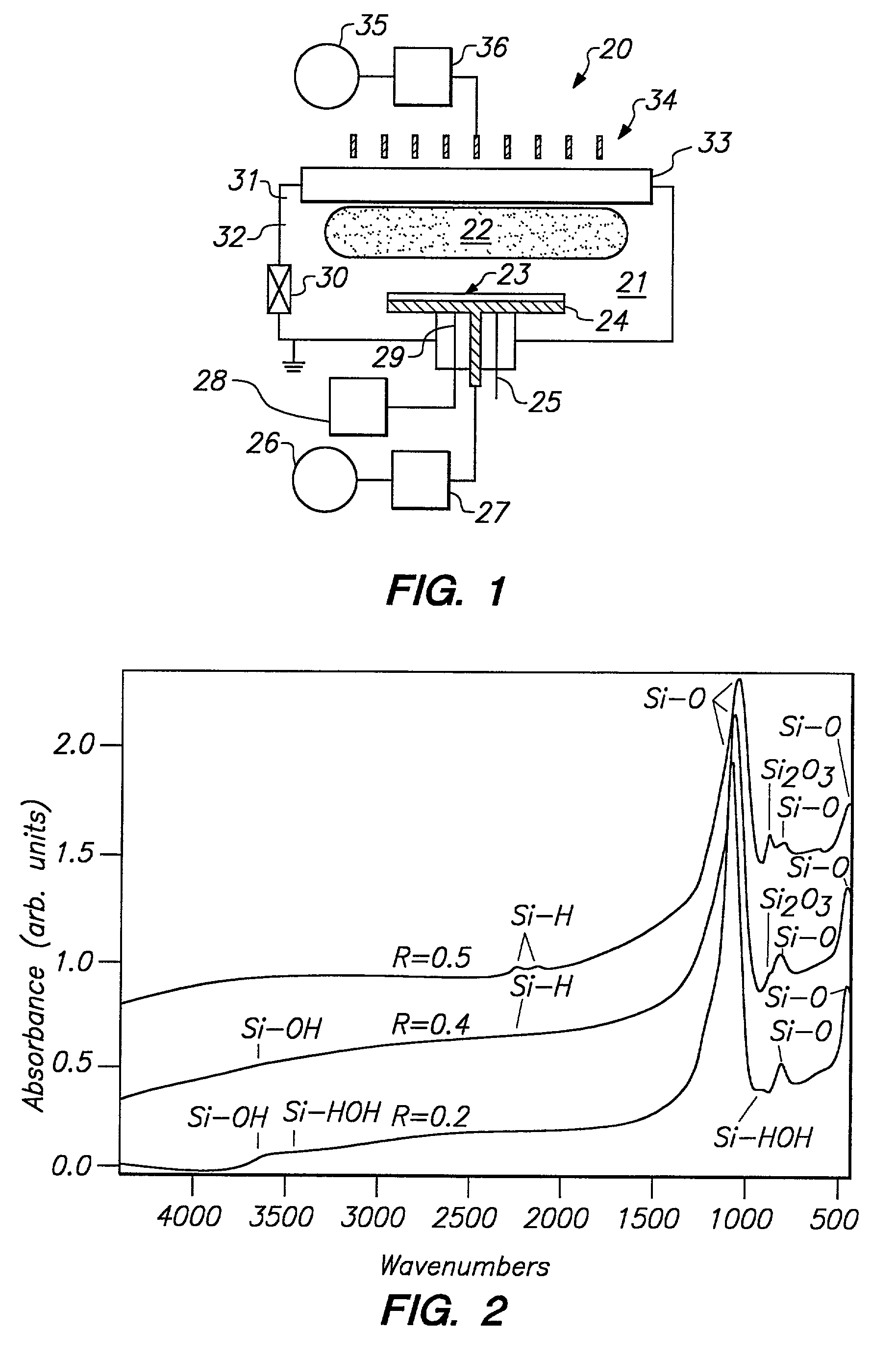
[0069] SiO.sub.2 IMD and capping depositions were conducted in an ICP system similar to that of FIG. 4. In this example 200 mm wafers were processed. The wafers were

[0070] In these depositions (0.5 .mu.m gaps), argon was included in the process gas.

[0071] However, the addition of argon is not always necessary as indicated in the preferred ranges. In the deposition of the cap layer, the initial deposition can employ a high electrode RF bias power to produce a good quality film. Thereafter, a lower bias power can be applied (preferably while maintaining about the same electrode temperature) to produce a sacrificial cap layer of lesser quality. Typically this sacrificial cap layer is substantially removed in a subsequent planarization process.

[0072] Generally a higher substrate temperature improves deposited film properties.

[0073] Typically, there are two primary contributors to the substrate temperature: (1) thermal heating from the substrate sup...


PUM

PropertyMeasurementUnit
frequencyaaaaaaaaaa
temperatureaaaaaaaaaa

Abstract

A method of depositing a dielectric film on a substrate in a process chamber of an inductively coupled plasma-enhanced chemical vapor deposition reactor. Gap filling between electrically conductive lines on a semiconductor substrate and depositing a cap layer are achieved. Films having significantly improved physical characteristics including reduced film stress are produced by heating the substrate holder on which the substrate is positioned in the process chamber.

Description

[0001] The present invention relates to a method and apparatus for high-density plasma-enhanced chemical vapor deposition of semiconducting and dielectric films and more particularly to techniques for depositing such films into high aspect ratio gaps on semiconductor substrates such as silicon wafers having metal interconnection layers.DESCRIPTION OF THE RELATED ART[0002] Chemical vapor deposition (CVD) is conventionally used to form various thin films in a semiconductor integrated circuit. CVD can form thin films such as SiO.sub.2, Si.sub.3N.sub.4, Si or the like with high purity and high quality. In the reaction process of forming a thin film, a reaction vessel in which semiconductor substrates are arranged can be heated to a high temperature condition of 500 to 1000.degree. C. Raw material to be deposited can be supplied through the vessel in the form of gaseous constituents so that gaseous molecules are thermally dissociated and combined in the gas and on a surface of the substr...

Claims


Application Information

Patent Timeline
Patent Type & Authority Applications(United States)
IPC IPC(8): C23C16/40C23C16/507H01L21/316H01L21/768
CPCC23C16/402C23C16/507H01J37/321H01L21/02126H01L21/02164H01L21/02211H01L21/02274H01L21/02301H01L21/02315H01L21/02362H01L21/31612H01L21/76837Y10S438/906Y10S438/902C23C16/40
Inventor SHUFFLEBOTHAM, PAUL KEVINMCMILLIN, BRIANDEMOS, ALEXNGUYEN, HUONGBERNEY, BUTCHBEN-DOR, MONIQUE
Owner SHUFFLEBOTHAM PAUL KEVIN
Why Eureka
Try Eureka