Nanoscale patterning for the formation of extensive wires

a technology of nanoscale and extensive wires, applied in the direction of photomechanical equipment, instruments, and semiconductor/solid-state device details, can solve the problems of limiting the advancement of lithographically defined patterning, affecting the placement of free-standing wires, and affecting the effect of lithographic accuracy

Inactive Publication Date: 2001-11-22
SAMSUNG ELECTRONICS CO LTD
View PDF0 Cites 29 Cited by
  • Summary
  • Abstract
  • Description
  • Claims
  • Application Information

AI Technical Summary

Problems solved by technology

With the constantly decreasing feature sizes of integrated-circuit devices, the need for increasingly fine, lithographically-defined patterning is limiting further advances of the technology.
However, Au and Fe migrate into Si rapidly and create deep levels, which can degrade devices, such as addressing circuitry and other portions of the system formed by conventional Si integrated-circuit technology.
However, it is difficult to control the placement of these free-standing wires, and therefore it is difficult to use these nanowires in real integrated circuits.
Also, the use of X-rays requires a synchrotron, and thus is very expensive.
In either event, it is not presently possible to achieve critical dimensions in patterning down to 10 nm.

Method used


Image

  • Nanoscale patterning for the formation of extensive wires

Examples


Embodiment Construction

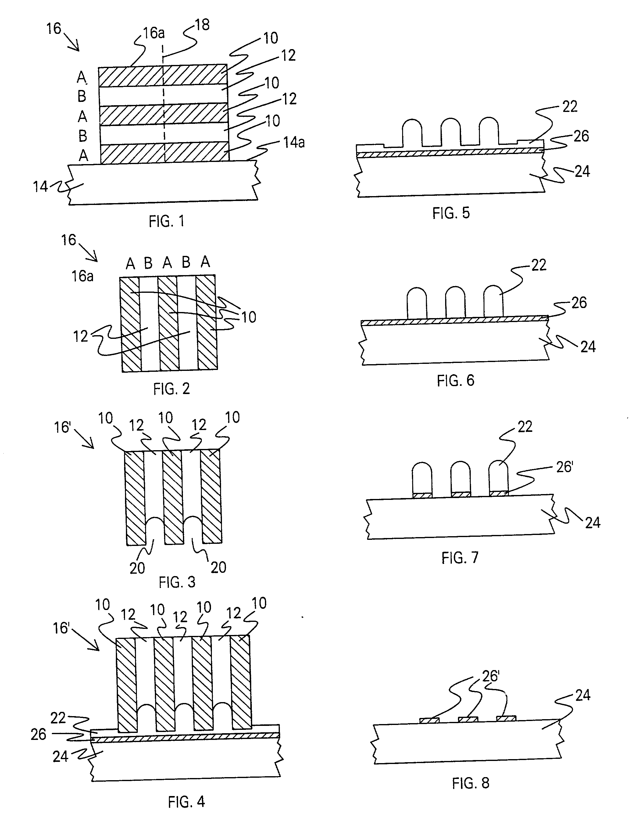
[0024] Nanoscale strips for device applications are fabricated by depositing composite thin films with different materials A and B, as illustrated in FIG. 1. Essentially, as described in greater detail below, a plurality of alternating layers of A material 10 and B material 12 are deposited on a major surface 14a of a substrate 14 to form a stack 16, also having a major surface 16a, parallel to the major surface of the substrate. Preferably, the material having the least lattice mis-match with the substrate 14 is deposited in order to keep a smooth growth surface and flat, sharp interfaces between materials 10 and 12.

[0025] The layers 10, 12 are then cleaved along a line 18 normal to the major surface 16a of the stack 16 to expose the cross-section, as shown in FIG. 2. Cleaving is performed by any conventional technique useful in cleaving a plurality of alternating layers of dissimilar materials. Such techniques are well-known in the art for the materials used for layers A and B, wh...


PUM

PropertyMeasurementUnit
depthaaaaaaaaaa
thicknessaaaaaaaaaa
thicknessaaaaaaaaaa

Abstract

A method for forming a platen useful for forming nanoscale wires for device applications comprises: (a) providing a substrate having a major surface; (b) forming a plurality of alternating layers of two dissimilar materials on the substrate to form a stack having a major surface parallel to that of the substrate; (c) cleaving the stack normal to its major surface to expose the plurality of alternating layers; and (d) etching the exposed plurality of alternating layers to a chosen depth using an etchant that etches one material at a different rate than the other material to thereby provide the surface with extensive strips of indentations and form the platen useful for molding masters for nano-imprinting technology. The pattern of the platen is then imprinted into a substrate comprising a softer material to form a negative of the pattern, which is then used in further processing to form nanowires. The nanoscale platen thus comprises a plurality of alternating layers of the two dissimilar materials, with the layers of one material etched relative the layers of the other material to form indentations of the one material. The platen is then oriented such that the indentations are parallel to a surface to be imprinted.

Description

[0001] The present application is related to application Ser. No. 09 / 280,048, entitled "Chemically Synthesized and Assembled Electronic Devices", filed on Mar. 29, 1999, which is directed to the formation of nanowires used for nanoscale computing and memory circuits. The present application is also related to applications Ser. No. 09 / 280,225, entitled "Molecular Wire Crossbar Interconnect (MWCI) for Signal Routing and Communications", Ser. No. 09 / 280,045, entitled "Molecular Wire Crossbar Logic (MWCL)", Ser. No. 09 / 280,189, entitled "Molecular Wire Crossbar Memory", and Ser. No. 09 / 280,188, entitled "Molecular Wire Transistor (MWT)", all also filed on Mar. 29, 1999, which are all directed to various aspects of memory and logic circuits utilized in nanocomputing.[0002] The present invention is generally directed to nanoscale computing and memory circuits, and, more particularly, to the formation of nanowires for device applications.[0003] With the constantly decreasing feature sizes ...

Claims


Application Information

Patent Timeline
Patent Type & Authority Applications(United States)
IPC IPC(8): B82B3/00G03F7/00H01L21/3213H01L21/768
CPCB82Y10/00B82Y40/00G03F7/0002H01L21/3213H01L21/76838Y10S977/887H01L21/02603H01L21/02532H01L21/02546H01L21/0262H01L21/02631
Inventor CHEN, YONGWILLIAMS, R. STANLEY
Owner SAMSUNG ELECTRONICS CO LTD
Why Eureka
Try Eureka