Probe device

a technology of probes and mount tables, applied in measurement devices, semiconductor/solid-state device testing/measurement, instruments, etc., to achieve the effects of enhancing the reliability of inspection, facilitating the control of the vertical and smooth movement of the mount tabl

Inactive Publication Date: 2002-01-31
KUJI MOTOHIRO +1
View PDF0 Cites 11 Cited by
  • Summary
  • Abstract
  • Description
  • Claims
  • Application Information

AI Technical Summary

Benefits of technology

0012] Specifically, the invention aims at always keeping, even if objects to be inspected increase in diameter in the future, the mounting table horizontal in inspections and always putting the contact terminals and the object in contact under uniform pressure, thereby enhancing the reliability of the inspection.
0013] The invention also aims at smoothly moving the mount table in the horizontal and vertical directions and controlling the vertical movement of the mount table very easily.

Problems solved by technology

To cope with this, conventional probe apparatuses have to solve various problems.

Method used


Image

  • Probe device
  • Probe device
  • Probe device

Examples


Embodiment Construction

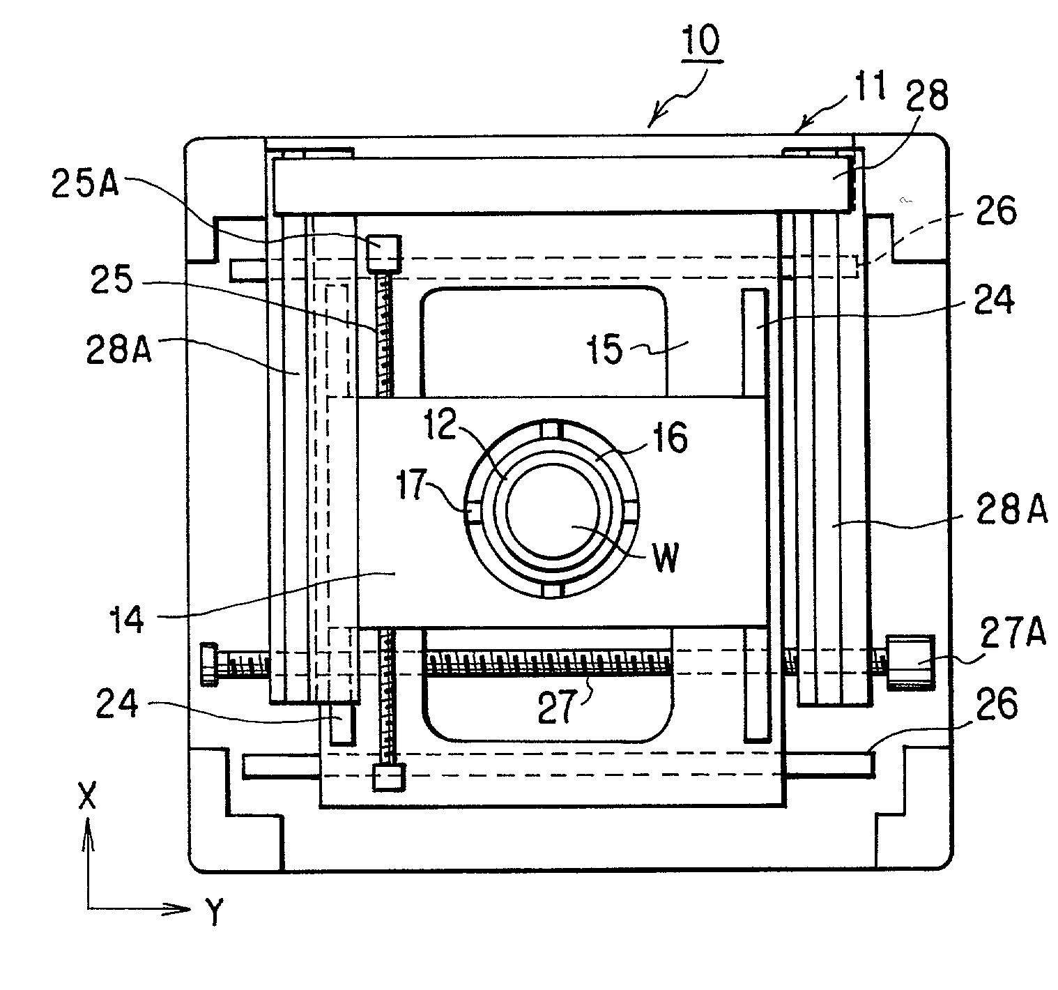
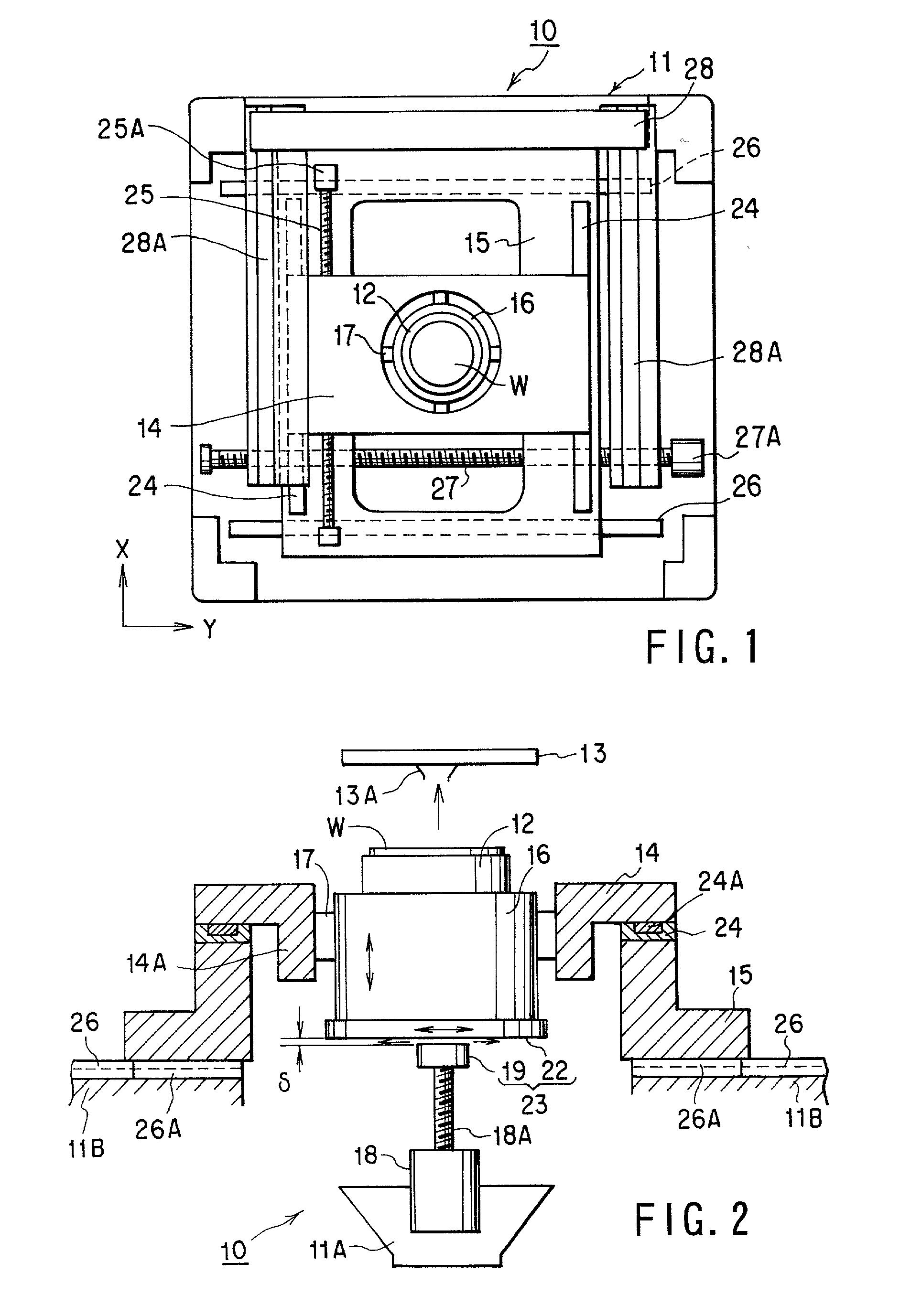
[0042] The present invention will now be described on the basis of embodiments shown in FIGS. 1 to 5. A probe apparatus 10 of the embodiment, as shown in FIGS. 1 and 2, is characterized by a vertical drive mechanism of a main chuck within a prober chamber 11. Specifically, a main chuck 12, on which a wafer W of, e.g. 12 inches is placed, is provided within the prober chamber 11 of the embodiment. A probe card 13 is fixed above the main chuck 12. The main chuck 12, as shown in FIGS. 1 and 2, is reciprocally moved in X- and Y-directions by a first stage (X-stage) 14 and a second stage (Y-stage) 15 and is vertically moved in an Z-direction by a Z-stage 16. Thereby, the wafer W placed on the main chuck 12 is put in electric contact with probe terminals 13A of the probe card 13. In this contact state, the electrical characteristics of the wafer W are inspected.

[0043] The drive mechanisms for the X-, Y- and Z-stages 14, 15 and 16 will now be described in detail.

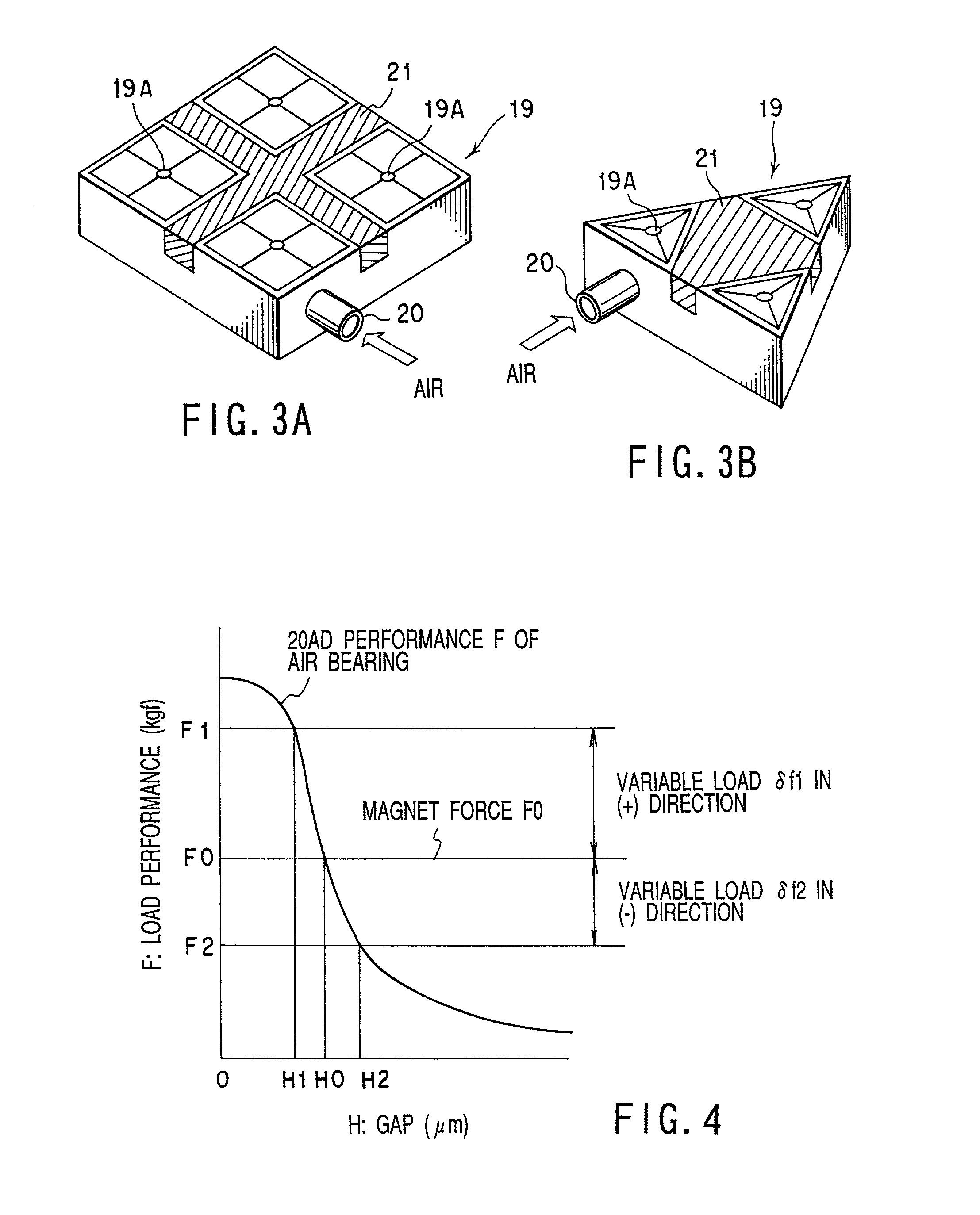
[0044] A cylindrical guide ...


PUM


Abstract

A probe apparatus 10 comprises a probe card 13, a main chuck 12, an X-stage 14 and a Y-stage 15. A vertical drive mechanism 18 is provided such that an extension line from a center for inspection of the probe card 13 coincides with an axis of the vertical drive mechanism. A static-pressure thrust air bearing 19, which is coaxial with the vertical drive mechanism 18 and vertically drives a main chuck 12, is provided as a vertically movable member. A gap-maintaining means 23 is provided to maintain a gap at a constant size between the static thrust air bearing 19 and the main chuck 12.

Description

[0001] The present invention relates to a probe apparatus, and more particularly to a probe card with a plurality of probe terminals which are put in contact with a plurality of electrodes of an object to be tested, thereby to test electrical characteristics of the object.[0002] FIGS. 6 and 7 show a conventional probe apparatus for testing electrical characteristics of semiconductor devices formed on a semiconductor wafer. The probe apparatus comprises a loader chamber 1 for pre-aligning a wafer W and feeding the wafer W, and a prober chamber 2 for receiving the wafer W from the loader chamber 1 and testing the electrical characteristics thereof. A probe card 7 is detachably attached to a head plate 8 which forms a top surface of the prober chamber 2.[0003] As is shown in FIG. 7, fork 3 and a sub-chuck 4 are provided in the loader chamber 1. While the wafer W is being carried by the fork 3, the wafer W is pre-aligned by the sub-chuck 4 with reference to its orientation flat.[0004] A...

Claims


Application Information

Patent Timeline
Patent Type & Authority Applications(United States)
IPC IPC(8): G01R31/28G01R1/06H01L21/66
CPCG01R31/2851G01R31/2887H01L22/00
Inventor KUJI, MOTOHIROAKAIKE, YUTAKA
Owner KUJI MOTOHIRO
Why Eureka
Try Eureka