Process for producing a laminated ink-jet recording head
- Summary
- Abstract
- Description
- Claims
- Application Information
AI Technical Summary
Benefits of technology
Problems solved by technology
Method used
Image
Examples
first embodiment
[0059] First Embodiment
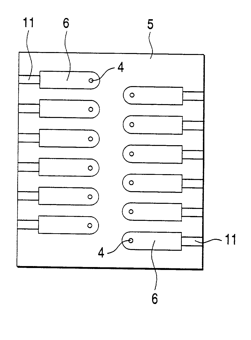
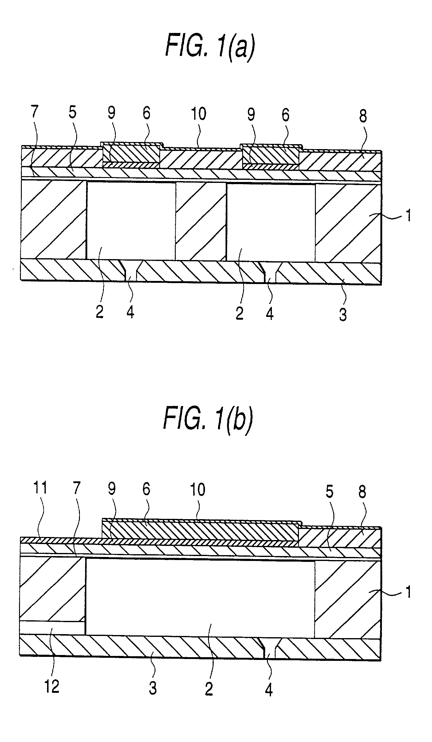
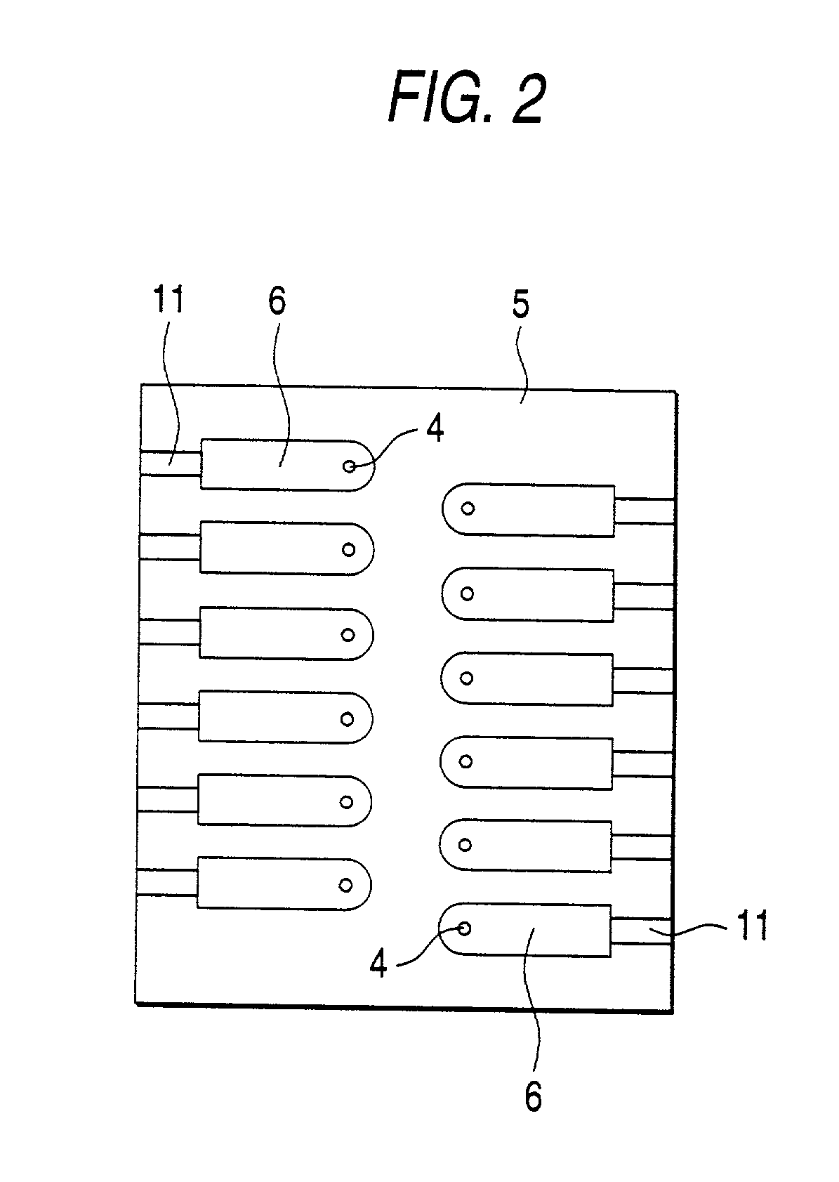
[0060] FIGS. 1(A) and (B) and FIG. 2 each show a first embodiment of the invention and in these drawings, numeral 1 signifies a spacer. The spacer is either made by performing anisotropic etching or chemical etching on a substrate, such as a single-crystal silicon substrate, a stainless steel substrate or the like, that have a film thickness (thickness) suitable for forming pressure generating chambers 2 in such a way that it is penetrated from one side to the other (from top to-bottom or from bottom to top as seen in FIG. 1(A)) or by press forming a ceramic green sheet and sintering it.
[0061] Numeral 3 signifies a nozzle plats. Nozzle orifices 4 are bored through the plate in positions that correspond to (communicate with) the pressure generating chambers 2. The plate is secured to one side of the spacer 1 by means of an adhesive or the like so as to provide an airtight condition.
[0062] Numeral 5 signifies a diaphragm that is made of a thin sheet elastic enou...
second embodiment
[0082] Second Embodiment
[0083] We next describe a second embodiment of the invention in accordance with the process shown in FIGS. 5 and 5. In this embodiment, description is made of the case where the spacer is formed of a single-crystal silicon substrate that can be etched anisotropically.
[0084] In the step shown in FIG. 5 (I) all surfaces of a single-crystal silicon substrate 40 are treated by a thermal oxidation method to form a silicon dioxide film 41. The silicon dioxide film 41 also functions as an etching protective film in a subsequent step.
[0085] Next, in the step shown in FIG. 5(II), an insulation film 43 is formed on the silicon single-crystal substrate 40 having the silicon dioxide film 41 formed thereon, in such a way that it has openings (windows) 42 in positions that correspond to pressure generating chambers 50.
[0086] Next, in the step shown in FIG. 5(III), a titanium layer 44 is formed on the surface of the silicon dioxide film 41 via the openings (windows) 42 form...
third embodiment
[0091] Third Embodiment
[0092] We next describe a third embodiment of the invention with reference to FIGS. 8(A) and 8(B).
[0093] in the drawings, numeral 61 signifies a titanium layer serving as a common lower electrode and this titanium layer 61 is formed in a film thickness of about 0.1 .mu.m by sputtering titanium on the entire surface of a diaphragm 62. Numeral 63 signifies an insulation layer formed on the surface of the diaphragm 62 and this insulation layer 63 is formed of an insulation material such as silicon dioxide (SiO.sub.2), polyimide or the like in a film thickness of about 1 .mu.m in such a way as to form openings (windows) in regions that correspond to pressure generating chambers 2.
[0094] Numeral 64 signifies a piezoelectric vibrating element, which is formed by growing a piezoelectric material on the titanium layer 61 serving as a substrate for growth by the hydrothermal method in such a film thickness (thickness) that its surface protrudes beyond the insulation la...
PUM
| Property | Measurement | Unit |
|---|---|---|
| thickness | aaaaa | aaaaa |
| thickness | aaaaa | aaaaa |
| thickness | aaaaa | aaaaa |
Abstract
Description
Claims
Application Information


