Solid-state imaging device and electronic camera and shading compensation method

a technology of imaging device and electronic camera, which is applied in the direction of radio frequency controlled devices, printers, instruments, etc., can solve the problems of complex task of writing a correction table based on these correction values (multiplication factors) to a rom before shipping, and can occur in the preshipment of shading correction, etc., to achieve the effect of optimum illuminance profile, accurate correction value, and excellent cost performan

Inactive Publication Date: 2002-02-28
NIKON CORP
View PDF3 Cites 74 Cited by
  • Summary
  • Abstract
  • Description
  • Claims
  • Application Information

AI Technical Summary

Benefits of technology

0025] Also, the solid-state imaging device may separately include a first output part for reading output signals from pixels in the effective pixel part and a second output part for reading output signals from pixels in the available pixel part. Through this it is possible to immediately obtain the data needed for finding the shading correction value.
0026] Also, the solid-state imaging may include a light-shielding film having a specific aperture formed at the plane of incidence side of the available pixel part, the center of the specific aperture being offset by a distance that is predetermined for each pixel from the center of a selected photoelectric conversion element. This makes it possible to compare luminance information between pixels at the light detection part after the light has been shielded by multiple light-shielding films, and makes it possible to find where on the photodiodes (photoelectric conversion elements) light is incident. Also, it is possible to find any slant in the angle of incidence of an incident light ray, and to use this result to find a shading correction value in situ.
0027] Also, the solid-state imaging device may include a microlens disposed at each pixel at the plane of incidence of photoelectric conversion elements in the light-receiving region. The microlenses of the available pixel part may be disposed so that their optical axes are offset by a fixed distance that is predetermined for each pixel from the center of the relevant or selected photoelectric conversion element. This makes it possible to compare luminance information between pixels at multiple light detection parts with different microlens positions, and it is possible to find where on the photodiodes (photoelectric conversion elements) light is incident. Also, it is possible to find any slant to the angle of incidence of an incident light ray, and to use this result to find a shading correction value in situ.
0028] Also, the solid-state imaging device may include a reference pixel that is in the available pixel part and does not have a microlens. This makes it possible to compare the luminance signal from a light detection part with pixels having microlenses to the luminance signal from a light detection part with pixels not having microlenses, thereby allowing a more accurate correction value to be obtained.
0029] Also, the solid-state imaging device may include a multiple types of color filters that are disposed at pixels in the available pixel part, and a signal may be output from the light detection part indicating the degree of shading at a pixel where a specific color filter is disposed. This makes it possible to find a shading correction value corresponding to the characteristics of each color filter.
0030] Also, an electronic camera described may be equipped with any of these solid-state imaging device. Such a camera may include an image adjustment means for adjusting image data based on the aforesaid signal indicating the degree of shading. The electronic camera may be a replaceable lens type of single lens reflex electronic camera. Therefore the amount of correction while taking a picture can be suitably determined based on the signal from the light detection part of the solid-state imaging device. Shading correction may be performed using a transmissivity control film such as an EC film, etc. while taking a picture, so the picture is taken with the transmissivity of the transmissivity control film controlled at the effective pixel part surface so as to produce the optimum illuminance profile. Alternatively, shading correction may be performed by applying this correction value to image data obtained by taking a picture. Or both may be combined. As a result, it is not necessary to measure the shading correction value for each individual camera before shipment and write the correction to a ROM. This provides an electronic camera that is excellent in both cost and performance.

Problems solved by technology

Nevertheless, various defects can occur in preshipment shading correction as described above.
For a replaceable lens type of single lens reflex electronic camera it is therefore difficult to obtain a shading correction value (multiplication factor) to be written to a ROM before shipping.
Also, the task of writing a correction table based on these correction values (multiplication factors) to a ROM is complicated because that data amount increases.
Also, if the subject of correction is widened to luminance shading and color shading in order to increase the performance of an electronic camera, the amount of data written increases, and the required measurement time lengthens, and this leads to an increase in manufacturing cost.
In light of all of these facts pertaining to shading as described above, measuring shading before shipment for each individual electronic camera and finding its correction value greatly increases the data to be written to a ROM and also dramatically increases the manufacturing cost.
In addition, with a replaceable lens type of single lens reflex electronic camera the correction values written to the ROM cannot accommodate new types of replacement camera lens products that are developed after shipment.
The user must do so every time the lens is replaced, etc., thereby making the electronic camera operation troublesome and is not practical.

Method used


Image

  • Solid-state imaging device and electronic camera and shading compensation method
  • Solid-state imaging device and electronic camera and shading compensation method
  • Solid-state imaging device and electronic camera and shading compensation method

Examples


first embodiment

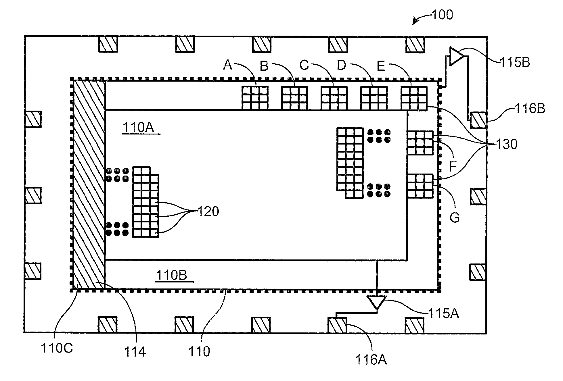
[0056] FIG. 1 is a drawing showing the overall structure of a solid-state imaging device 100 in accordance with a first embodiment. The solid-state imaging device 100 has a light-receiving region 110 (in the drawing, indicated by a thick broken line) having a central part that is an effective pixel part 110A and an available pixel part 110B surrounding the effective pixel part 110A. "Available pixel (part)" is generally defined as a concept that includes "effective pixel (part)," but in this application, "available pixel part" is defined for convenience as the "light-receiving region" excluding the "effective pixel part."

[0057] Also, an optical black region 110C for measuring dark current is provided near the effective pixel part 110A (at the left side in FIG. 1). This optical black region 110C is formed of pixels (not shown in the drawing) with the same structure as those in the effective pixel part 10A, and the plane of incidence of photodiodes (photoelectric conversion elements) ...

second embodiment

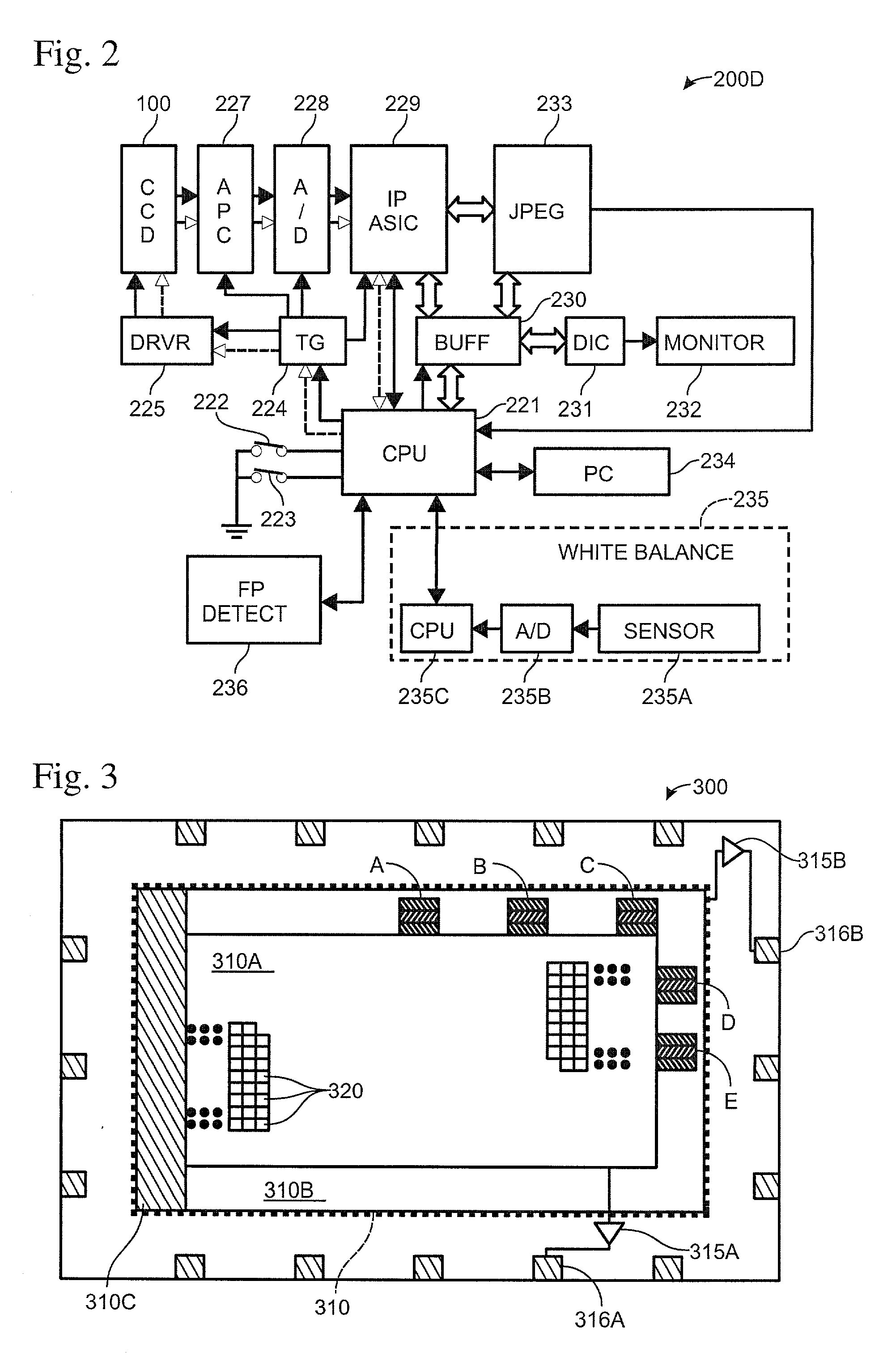
[0080] FIGS. 3-6 illustrate as a second embodiment a solid-state imaging device 300 which differs from the first embodiment in that a light-shielding film 332 having apertures 332a is formed at the plane of incidence of pixels 330 in an available pixel part 310B.

[0081] As shown in FIG. 3, the light-receiving region 310 is divided into an effective pixel part 310A and an available pixel part 310B. An optical black region 310C for measuring dark current is provided at a location near the effective pixel part 310A (at the left side in FIG. 3). Also, output amps 315A and 315B and pad electrodes 316A and 316B are formed outside the periphery (in the drawing, indicated by a thick broken line) of the light-receiving region 310. Output amps 315A and 315B amplify the output signals (voltage) of each of pixels 320 and 330 in the effective pixel part 310A and available pixel part 310B, respectively, and pad electrodes 316A and 316B allow the output signals to be read.

[0082] The available pixel...

third embodiment

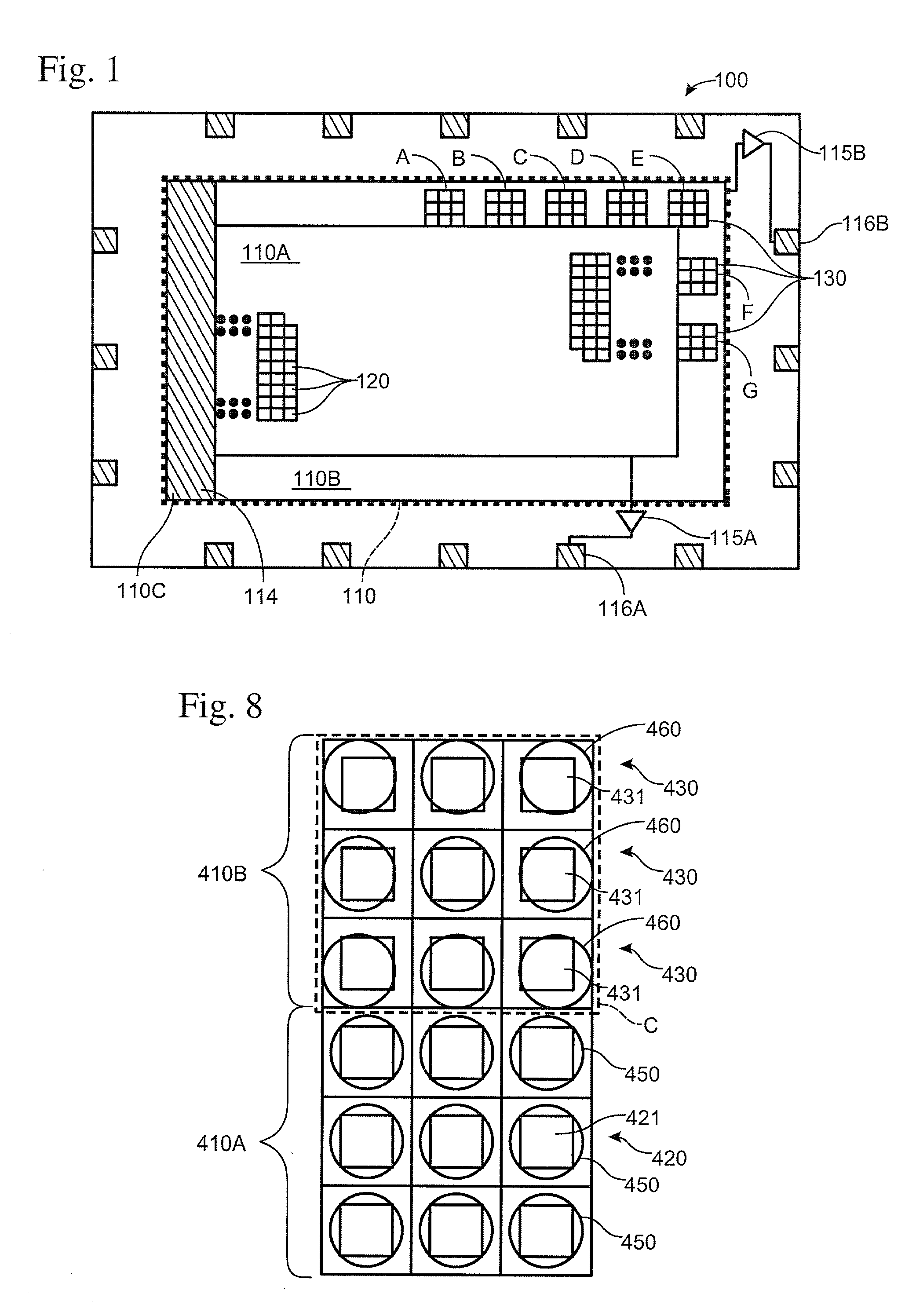
[0090] FIGS. 7-10 illustrate as a third embodiment a solid-state imaging device 400 which differs from the first embodiment in that microlenses 450 are disposed at the plane of incidence of pixels 420 in the effective pixel part 410A provided in the light-receiving region 410, and microlenses 460 are disposed at the plane of incidence of pixels 430 in the available pixel part 410B.

[0091] As shown in FIG. 7, the light-receiving region 410 of solid-state imaging device 400 is divided into an effective pixel part 410A and an available pixel part 410B. An optical black region 410C for measuring dark current is provided at the left side of the effective pixel part 410A in FIG. 7.

[0092] Also, output amps 415A and 415B and pad electrodes 416A and 416B are formed outside the periphery (in the drawing, indicated by a thick broken line) of the light-receiving region 410. Output amps 415A and 415B amplify the output signals (voltage) of each of pixels 420 and 430 in the effective pixel part 41...


PUM


Abstract

A solid-state imaging device provides an in situ shading correction value regardless of electronic camera performance variation or type of replacement lens installed, etc. In one implementation, light-receiving region 110 of a solid-state imaging device 100 is divided into an effective pixel part 110A and an available pixel part 110B. Pixels 130 in the available pixel part 110B provide output signals indicating the degree of shading at the effective pixel part 110A. Output signals from pixels 130 are used by a control part 220D of the electronic camera for shading correction of image data obtained by the effective pixel part 110A.

Description

[0001] The present invention pertains to a solid-state imaging device and an electronic camera. More specifically, the invention relates to a solid-state imaging device with a large imaging area that can suitably perform shading correction and to an electronic camera incorporating such a solid-state imaging device.BACKGROUND AND SUMMARY[0002] Conventionally known solid-state imaging devices for electronic cameras include CCD-type image sensor, CMOS-type image sensor, amplifier-type image sensor, etc. FIG. 21 shows a conventional CCD-type image sensor 10. As shown in the drawing, the CCD-type image sensor 10 consists of a plurality of pixels 12, vertical transfer electrode 13, horizontal transfer electrode 14, and output amp 15 formed on a semiconductor substrate 11. A charge generated by a photodiode (photoelectric conversion element) 12a (FIGS. 22, 23) of pixel 12 passes through the vertical transfer electrode 13, horizontal transfer electrode 14, and output amp 15 and is read outs...

Claims


Application Information

Patent Timeline
Patent Type & Authority Applications(United States)
IPC IPC(8): G03B17/48H01L27/14H01L27/146H01L27/148H04N5/335H04N5/361H04N5/369H04N5/372H04N5/374H04N5/378H04N9/07
CPCG03B17/48H01L27/14603H01L27/14621H01L27/14623H01L27/14627H01L27/14843H04N5/2254H04N5/3572H04N9/045H04N25/61H04N25/611
Inventor SUZUKI, SATOSHI
Owner NIKON CORP
Why Eureka
Try Eureka