

Optical-based sensing devices
a sensing device and optical technology, applied in the field of optical sensing devices, can solve problems such as excitation of fluorescen
- Summary
- Abstract
- Description
- Claims
- Application Information
AI Technical Summary
Problems solved by technology
Method used
Image

Examples
first embodiment
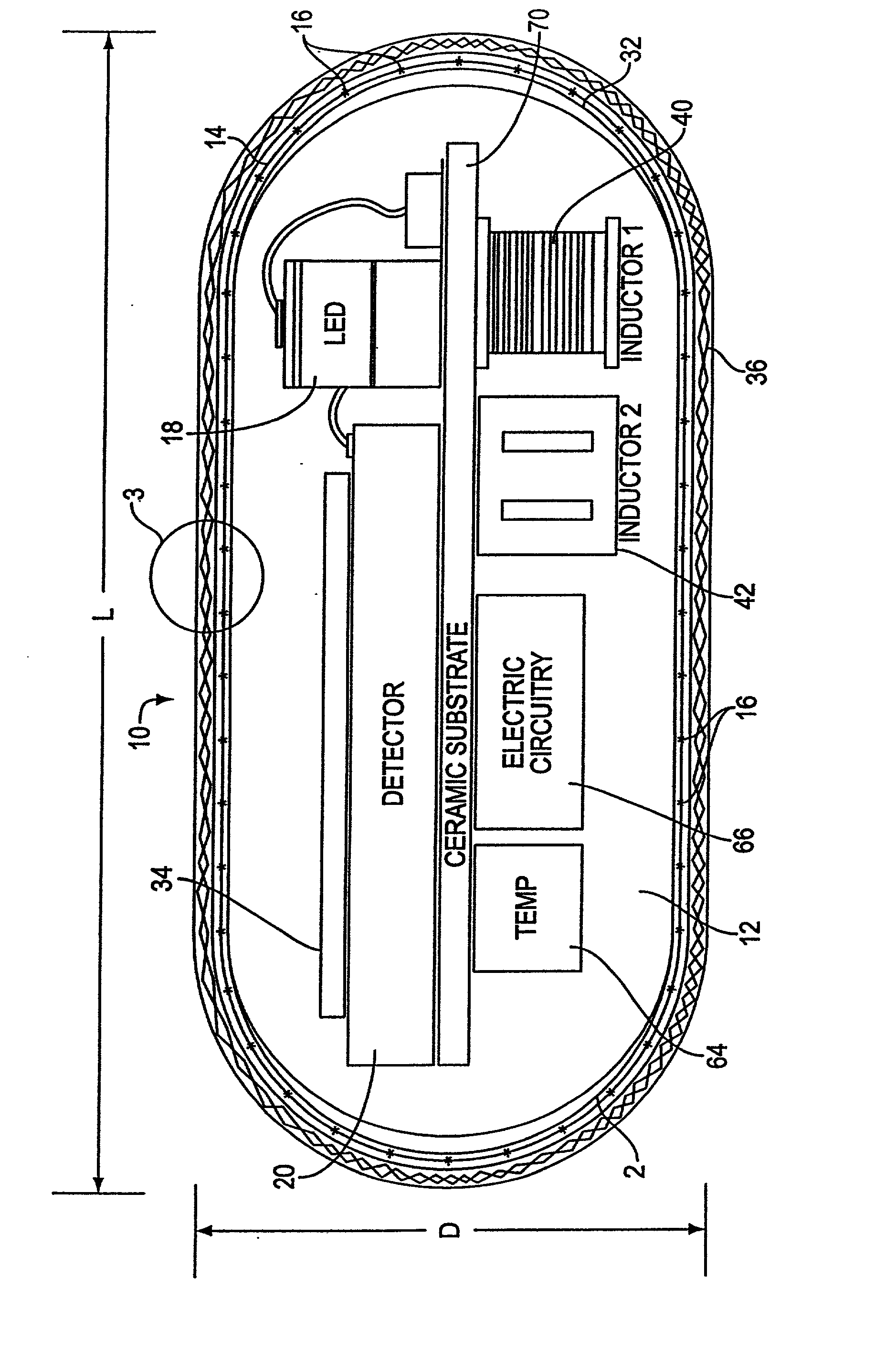
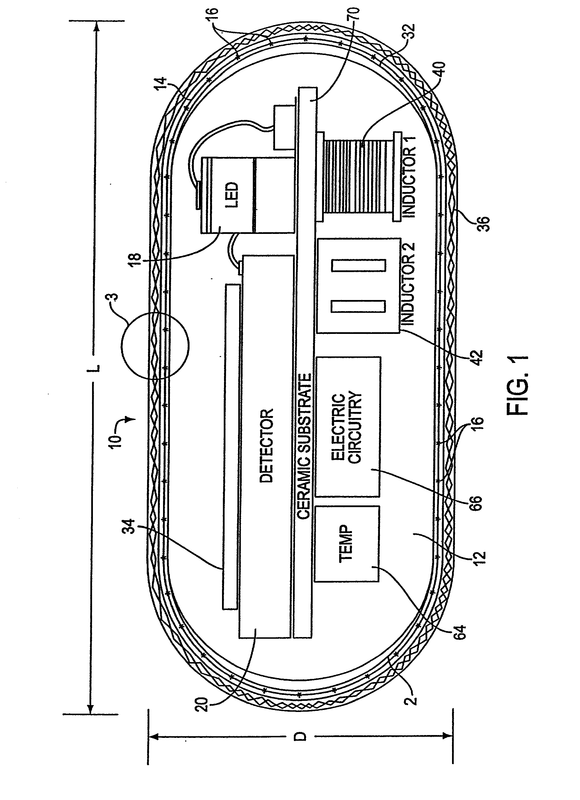
[0144] FIGS. 14(A)-14(B) illustrate a sensor 10 incorporating an optical reference channel. As shown, the sensor 10 preferably includes: a sensor body 12; an indicator membrane 14' having fluorescent indicator molecules distributed throughout the membrane; a reference membrane 14" having fluorescent control indicator molecules distributed throughout the membrane; a radiation source 18, such as for example a single LED similar to that described herein-above; an indicator channel photosensitive element 20-1, made, for example, similar to photosensitive element 20 described herein-above; a similar reference channel photosensitive element 20-2; a circuit substrate 70 (shown schematically with exemplary circuit elements 70i mounted thereto); a power source 40, such as for example an inductive power coil as shown; and a transmitter 42 such as for example a transmitter coil as shown. In any of the embodiments described herein, the membranes 14' and 14" can be made, for example, with materi...
second embodiment
[0168] Once again, the arrangement of the parts within the sensor can also be varied by those in the art. For example, FIGS. 17(C)-17(D) show a second embodiment similar to the embodiment shown in FIGS. 17(A)-17(B) with the indicator membrane 14' and the reference membrane 14" on the same side of the circuit board 70 and with a single radiation source, e.g., LED, 18--similar to the embodiments shown in FIGS. 14(A)-14(C). All of the applicable variations described above with respect to FIGS. 14(A)-14(C) and to FIGS. 17(A)-17(B) could be applied to the embodiment shown in FIGS. 17(C)-17(D).
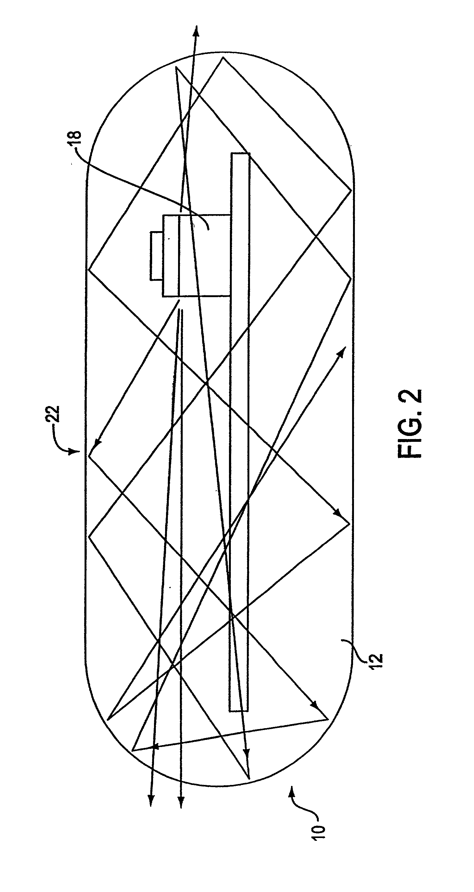
[0169] As another example, FIGS. 17(E)-17(F) show another embodiment similar to the embodiment shown in FIGS. 17(A)-17(C) with the indicator membrane 14' and the reference membrane 14" on the same side of the circuit board 70 but with two radiation sources, e.g., LEDs, 18-1 and 18-2 similar to the embodiments shown in FIGS. 15(A)-15(C) but with the LEDs spaced further apart in the illustrated exampl...
PUM
| Property | Measurement | Unit |
|---|---|---|
| diameter | aaaaa | aaaaa |
| length | aaaaa | aaaaa |
| length | aaaaa | aaaaa |
Abstract
Description
Claims
Application Information