System modules with atomic resolution storage memory

a technology of atomic resolution and memory, applied in the field of semiconductors, can solve the problems of inherent inefficiency of the arrangement of a microprocessor and a memory storage devi

Inactive Publication Date: 2002-06-06
HEWLETT PACKARD DEV CO LP
View PDF0 Cites 2 Cited by
  • Summary
  • Abstract
  • Description
  • Claims
  • Application Information

AI Technical Summary

Problems solved by technology

As may be readily apparent from the foregoing, assembly of such an arrangement of a microprocessor and a memory storage device suffers from inherent inefficiencies.

Method used


Image

  • System modules with atomic resolution storage memory
  • System modules with atomic resolution storage memory
  • System modules with atomic resolution storage memory

Examples


Embodiment Construction

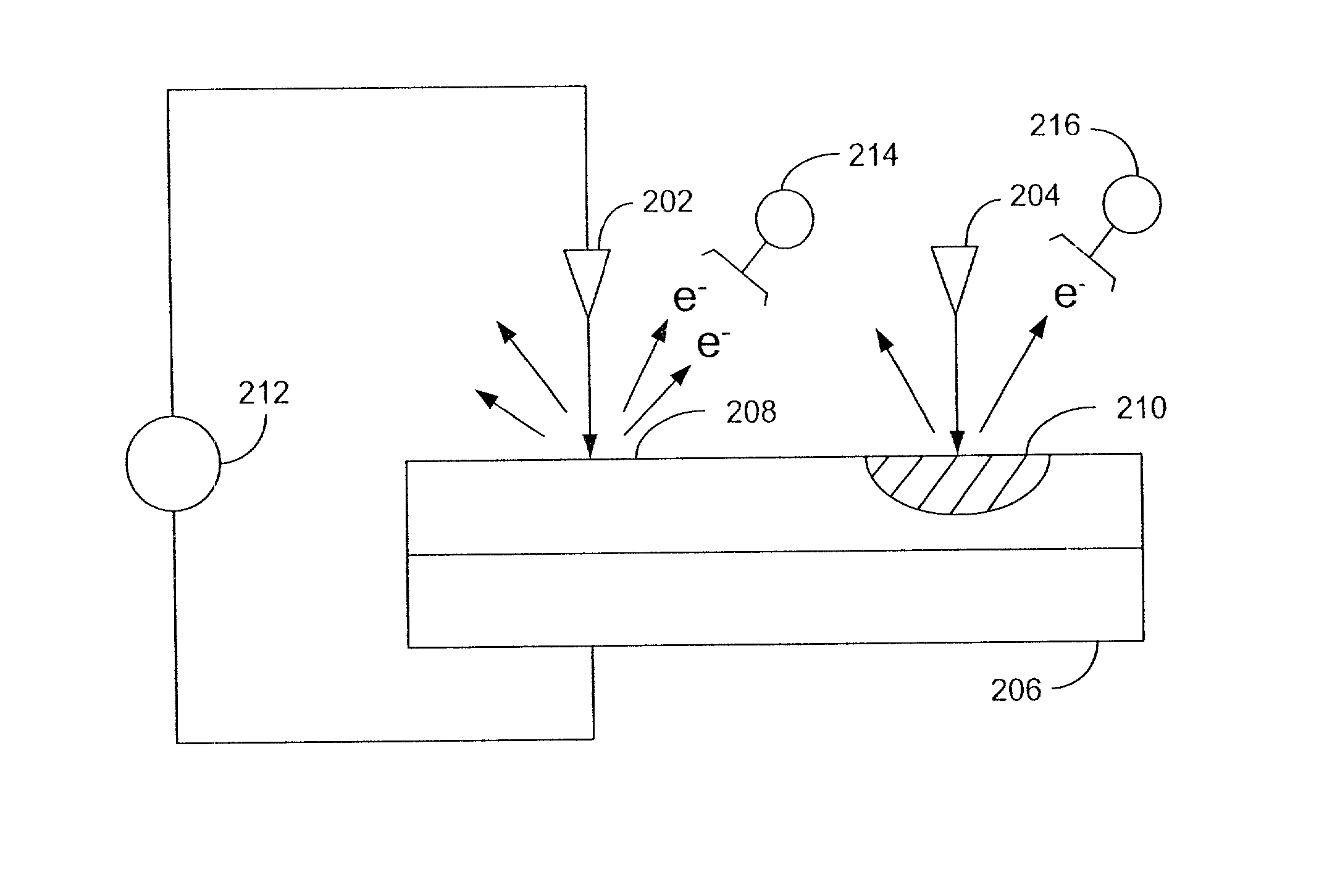
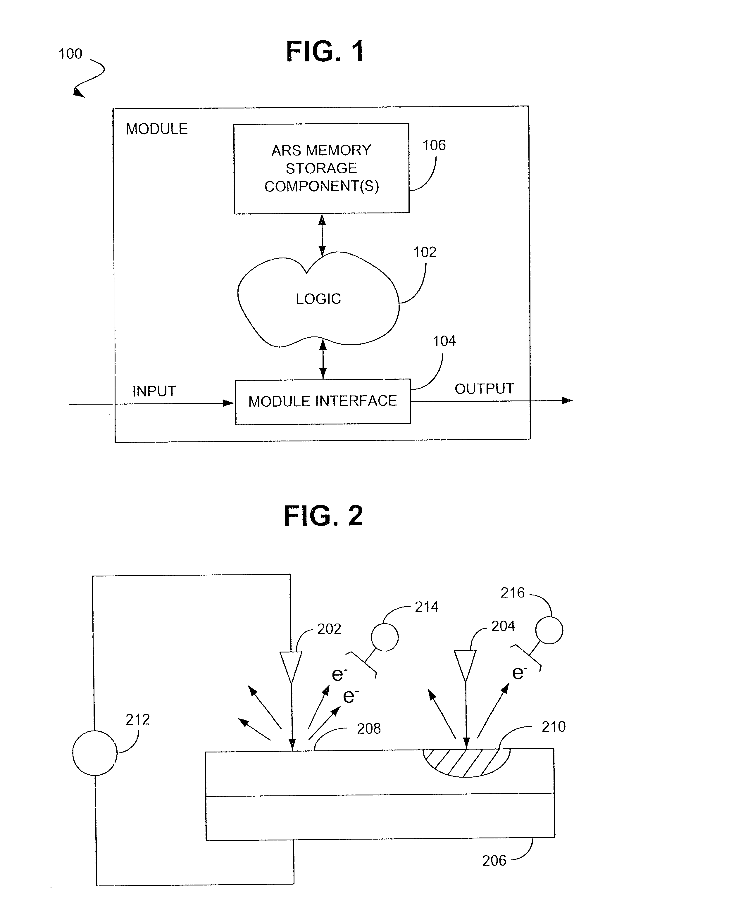
[0019] Reference will now be made to the drawings wherein like numerals indicate corresponding parts throughout the several views. As shown in FIG. 1, a preferred embodiment of the system module 100 of the present invention includes logic 102 which is utilized for performing various logic functions of the module. Logic 102 may be provided in various configurations and may be adapted for providing functionality of virtually limitless applications depending upon the configuration utilized. For example, and not for the purpose of limitation, the logic may be configured to function as a microprocessor.

[0020] Logic 102 is communicatively coupled with a module interface 104 that facilitates communication of components internal to the module with components external to the module. Additionally, logic 102 is communicatively coupled with memory storage component(s) 106 for facilitating storage and retrieval of data, such as by utilizing ARS technology (representative examples of which are de...


PUM

PropertyMeasurementUnit
electrical communicationaaaaaaaaaa
areasaaaaaaaaaa
power densityaaaaaaaaaa

Abstract

A preferred microprocessor module includes a first wafer incorporating a storage medium. The storage medium is provided with storage areas that are configurable in one of a plurality of structural states to represent information stored in the storage areas. A second wafer is arranged proximate the first wafer and includes electron beam emitters that are configured to electrically communicate with the storage medium. The storage medium and the emitters are configured to move relative to each other so that each emitter may provide a beam of electrons to at least one of the storage areas. Additionally, a third wafer is provided which includes logic circuitry configured to enable extraction of data from the storage areas of the storage medium and execution of instructions embodied within the data. Processor-based systems also are provided.

Description

[0001] 1. Field of the Invention[0002] The present invention generally relates to semiconductors and, more specifically, to semiconductor modules and systems employing atomic resolution storage (ARS) techniques.[0003] 2. Background of the Invention[0004] Memory storage devices employing ARS technology include a number of electron field emitters that are adapted to write data to and read data from various storage areas of a storage medium. During operation, a predetermined potential difference is applied between a field emitter and a corresponding gate that extracts an electron beam current from the emitter towards the storage area. Writing of data from an emitter to a storage area is accomplished by temporarily increasing the power density of the electron beam current to modify the structural state of the surface of the storage area. In contrast, reading data from the storage area is accomplished by observing the effect of the storage area on the electron beam of the emitter, or the...

Claims


Application Information

Patent Timeline
Patent Type & Authority Applications(United States)
IPC IPC(8): G11B9/00
CPCB82Y10/00G11B9/1418G11B9/14
Inventor CARTER, TIMOTHY L.
Owner HEWLETT PACKARD DEV CO LP
Why Eureka
Try Eureka