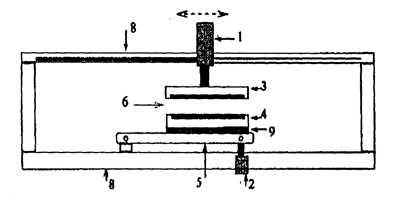
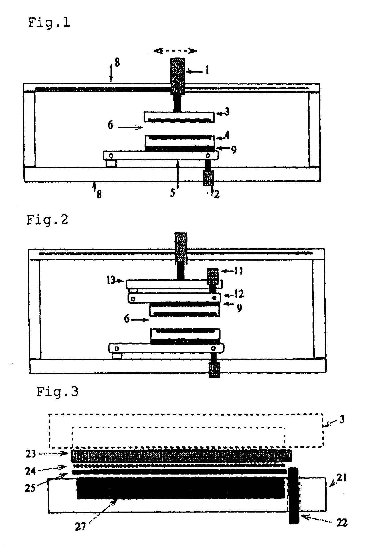
Separating machine for thinned semiconductor substrate and separation method
a technology of semiconductor substrate and separation method, which is applied in the direction of semiconductor/solid-state device manufacturing, basic electric elements, electric devices, etc., can solve the problems of method not being able to endure gold vapor deposition or the like, easy cracking of ceramics,
- Summary
- Abstract
- Description
- Claims
- Application Information
AI Technical Summary
Problems solved by technology
Method used
Image

Examples
example 1
[0053] There was prepared a semiconductor substrate made of a silicon wafer, which semiconductor substrate had aluminum thin film patterns and pads on its surface, had a silicon nitride layer as an insulating material and had a thickness of 0.625 mm and a diameter of 125.0 mm.
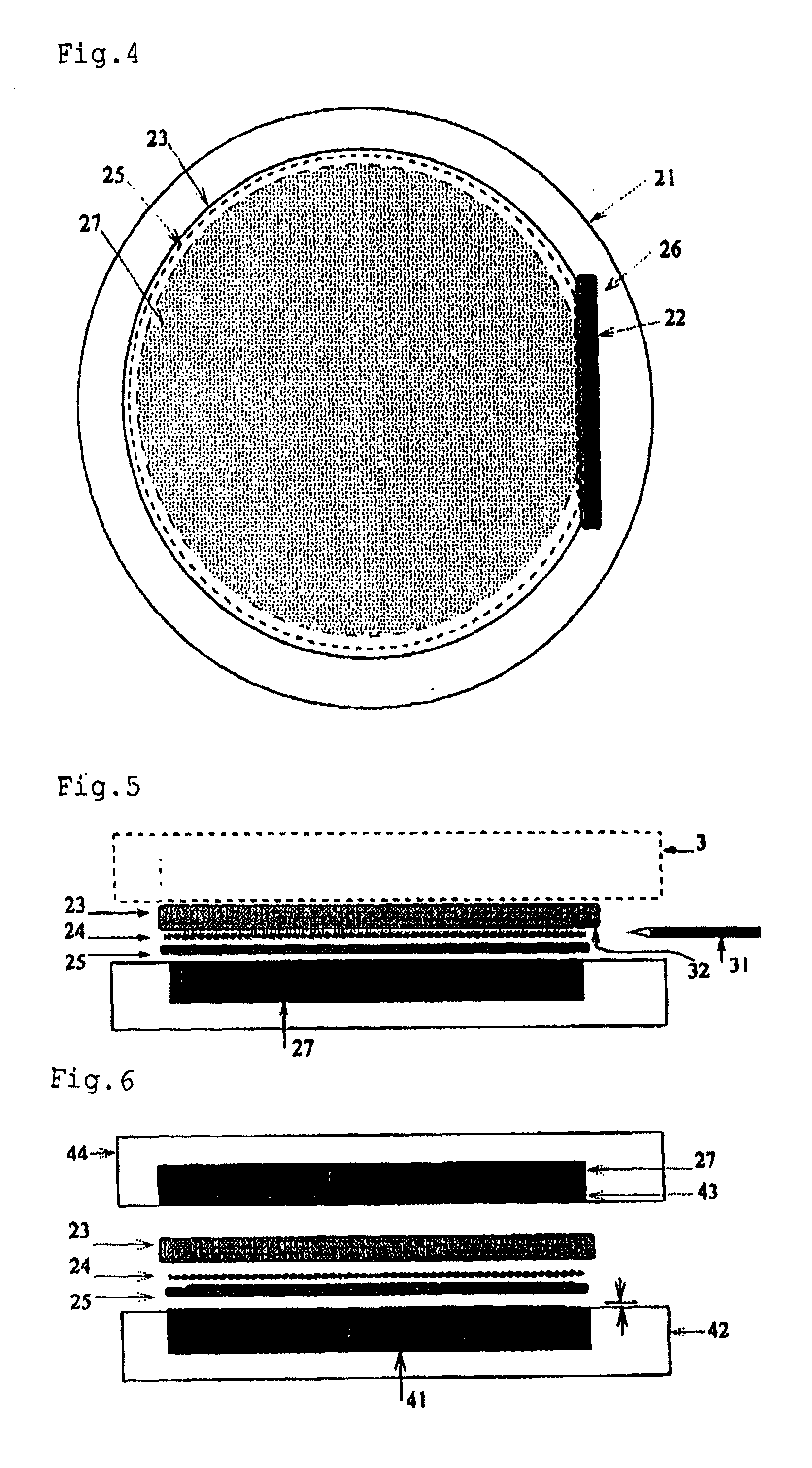
[0054] A disk of an aluminum nitride-boron nitride porous sintered body which disk had a board thickness of 0.625 mm and a diameter of 125.5 mm was surface-treated by pyrolysis of an organoaluminum compound to improve the compatibility with a resin to be impregnated, the surface-treated disk was impregnated with a resin, the impregnated-resin was cured by vacuum press and the surface of the resin-cured disk was polished so as to attain a surface roughness Ra=0.3 .mu.m, to prepare a holding substrate. A 25 .mu.m thick polyimide film having thermoplastic polyimide layers on both surfaces thereof (trade name: Upilex VT441S, supplied by Ube Industries, Ltd) was temporarily bonded to one surface of the holding subst...
example 2
[0065] The semiconductor substrate used in Example 1 was replaced with a semiconductor substrate having a thickness of 0.625 mm and a diameter of 150.0 mm and having an oxide layer as an insulating layer. The raw material for the holding substrate used in Example 1 was replaced with an aluminum nitride-boron nitride porous sintered body having a thickness of 0.625 mm and a diameter of 150.5 mm. A groove having a width of 5 mm and a depth of 25 .mu.m was made in the holding substrate in a position corresponding to the orientation-flat portion of the silicon wafer. The same polyimide film in kind as that in Example 1 was embedded in the groove and the same polyimide film in kind was temporally attached to the entire surface. The frame used in Example 1 was replaced with a frame having a size corresponding to these sizes. The medium-pressure setting of the medium-pressure cylinder of the hot press for bonding in Example 1 was changed from 2 MPa to 2.4 MPa. The press pressure in Example...
example 3
[0068] The semiconductor substrate used in Example 1 was replaced with a semiconductor substrate which had gold thin film patterns and pads on the surface of a gallium-arsenic wafer, had a polyimide layer as an insulating layer and had a board thickness of 0.625 mm and a diameter of 100.0 mm. Further, the holding substrate used in Example 1 was replaced with a holding substrate obtained by surface-treating an aluminum oxide-boron nitride porous sintered body disk having a board thickness of 0.625 mm and a diameter of 125.0 mm by pyrolysis of an organoaluminum compound, impregnating the surface-treated disk with a resin, curing the impregnated resin by vacuum press and polishing the surface of the disk until the surface roughness Ra became 0.3 .mu.m. A thermoplastic polyamide resin (nylon 6) having a thickness of 25 .mu.m was temporally attached to one surface of the above-obtained holding substrate. Further, the thinning was carried out by grinding and CMP until the thickness became...
PUM
 Abstract
Description
Claims
Application Information
 - Generate Ideas
- Intellectual Property
- Life Sciences
- Materials
- Tech Scout
- Unparalleled Data Quality
- Higher Quality Content
- 60% Fewer Hallucinations
Browse by: Latest US Patents, China's latest patents, Technical Efficacy Thesaurus, Application Domain, Technology Topic, Popular Technical Reports.
© 2025 PatSnap. All rights reserved.Legal|Privacy policy|Modern Slavery Act Transparency Statement|Sitemap|About US| Contact US: help@patsnap.com