Display device and method for manufacturing the same

Active Publication Date: 2002-09-26
138 EAST LCD ADVANCEMENTS LTD
View PDF10 Cites 21 Cited by
  • Summary
  • Abstract
  • Description
  • Claims
  • Application Information

AI Technical Summary

Benefits of technology

0021] In particular, by disposing the parts downstream from the light-receiving elements on one surface of a transparent substrate, disposing the parts upstream from the signal transmission lines on the other surface of the transparent

Problems solved by technology

As a result, EMI (electromagnetic interference) and skew between a plurality of ICs comprising th

Method used


Image

  • Display device and method for manufacturing the same
  • Display device and method for manufacturing the same
  • Display device and method for manufacturing the same

Examples


first embodiment

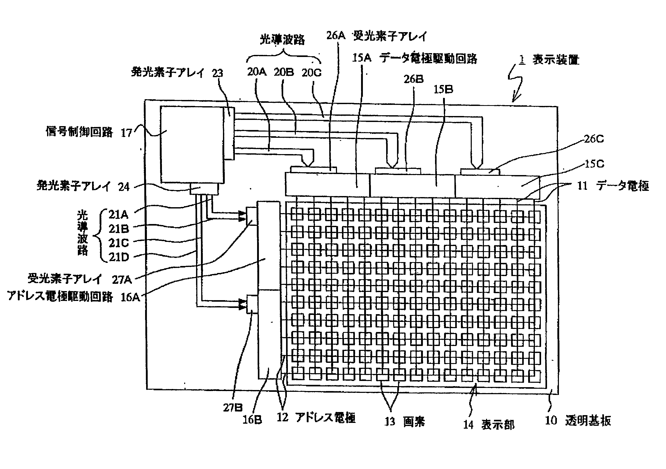
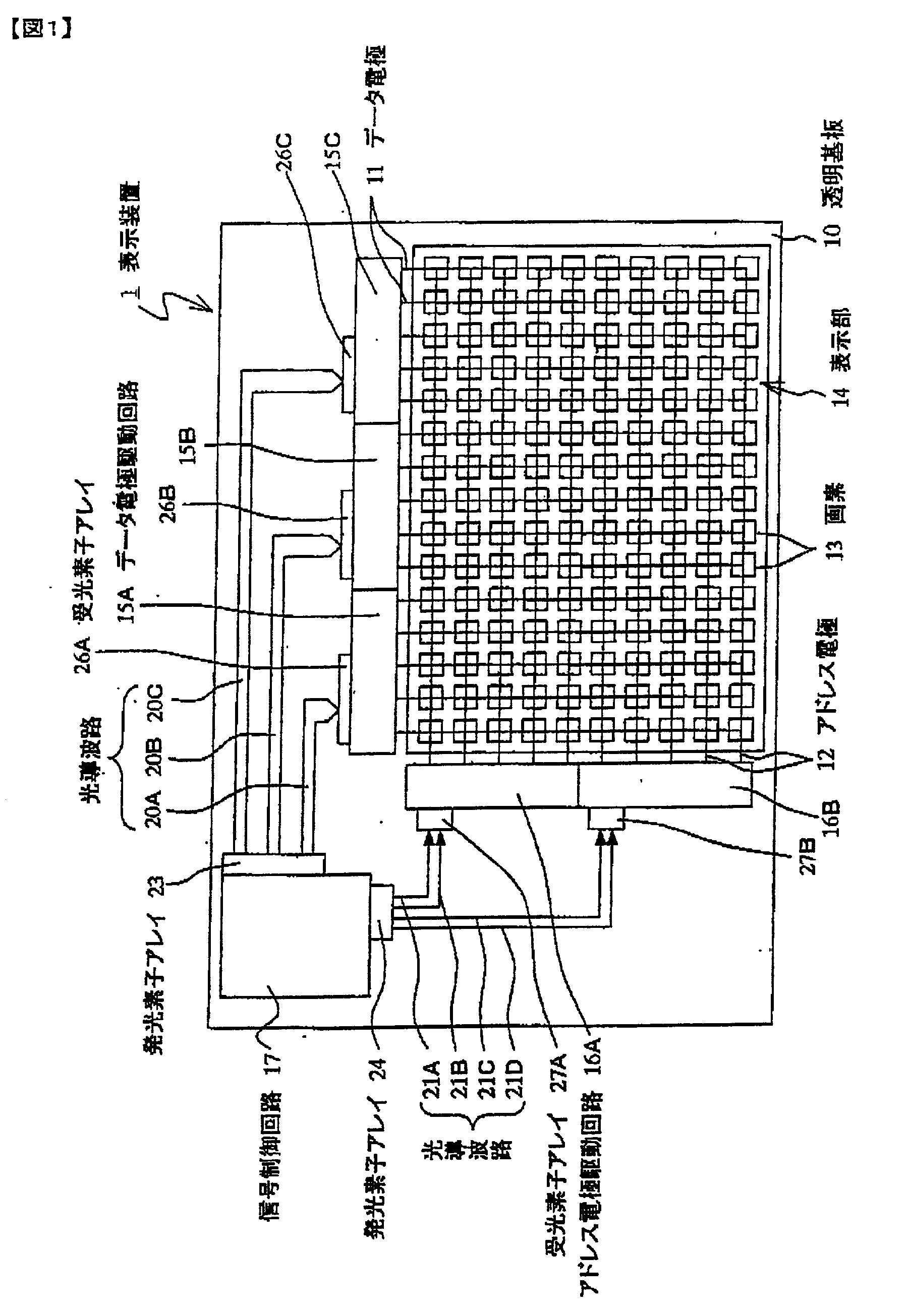
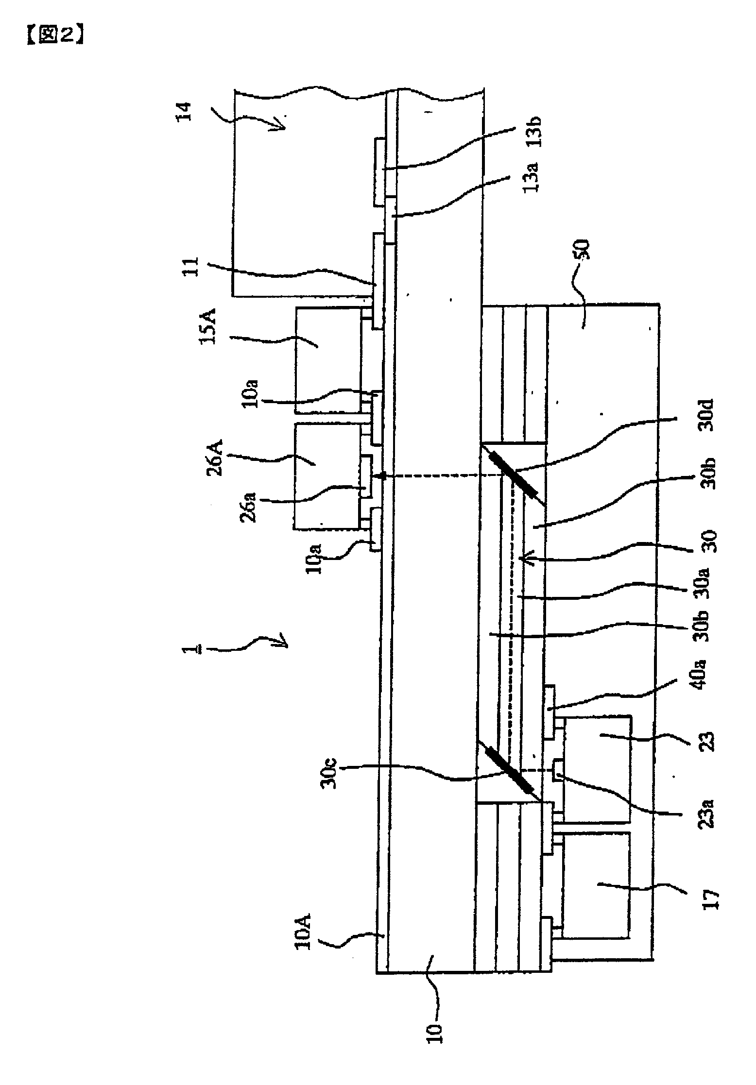
[0027] FIGS. 1 to 3 show the present invention FIG. 1 is a plan view showing the overall structure of a display device 1 and FIG. 2 is a sectional view of a principal part of the display device 1.

[0028] Specifically, the display device 1 is used for, for example, a display of a personal computer and preferably serves as a thin film transistor liquid crystal display device and an organic EL (electroluminescence) display device.

[0029] A plurality of data electrodes 11 extending in the longitudinal direction and a plurality of address electrodes 12 extending in the transverse direction are disposed in a grid on a transparent substrate 10. A display section 14 is formed in which pixels 13 are arrayed at respective intersections of the data electrodes 11 and the address electrodes 12. The structure of the pixels 13 are not specifically shown in the drawings, and have the same structure as in known liquid crystal display devices or organic EL display devices.

[0030] The data electrodes 11 ...

second embodiment

[0063] This embodiment is different from the second embodiment in that the data electrodes 11 are connected to the data electrode driving circuits 15A with a ribbon cable 64 because the data electrodes 11 are not formed on the substrate 10 but another transparent substrate 60.

[0064] Although FIG. 6 does not show the connection of the address electrodes 12 with the address electrode driving circuits 16, it is the same as in the second embodiment and the description is not repeated.

[0065] The data electrode driving circuits 15A to 15C control potentials of the data electrodes 11 connected thereto with the ribbon cables 64, and the address electrode driving circuits 16A and 16B drive the TFD elements 13a connected thereto with the address electrodes 12. Specifically, when a TFD element 13a connected with an address electrode 12 is driven by the address electrode driving circuits 16A or 16B, the pixel electrode 13b and the data electrode 11 connected to the TFD element 13a are electrica...

third embodiment

[0068] In this embodiment, as in the third embodiment, since the display electrodes 71 are disposed on the transparent substrate 70, the display electrodes 71 are connected to the display electrode driving circuits (data electrode driving circuits in FIG. 1) 15A with the ribbon cable 64.

[0069] Although FIG. 7 does not show the connection of the address electrodes 12 with the address electrode driving circuits 16, the connection is the same as in the second embodiment and the description is not repeated.

[0070] A voltage is applied to the address electrodes 12 and the display electrodes 71, thereby causing discharge (surface discharge) in the discharging chambers 13c to generate ultraviolet light. The fluorescent phosphor 13e is exposed to this ultraviolet light and thus the pixels 13 emit light.

[0071] FIG. 5 shows a fifth embodiment of the present invention. FIG. 5(a) is circuits diagram showing the interior structure of the signal control circuits 17, and FIG. 5(b) is circuits diagr...


PUM


Abstract

To provide a display device whose size and resolution can easily be increased. Signal transmission lines from a signal control circuits 17 to data electrode driving circuits 15A to 15C are optical waveguides 20A, 20B, and 20C serving as optical transmission lines capable of transmitting optical signals. Signal transmission lines from the signal control circuits 17 to address electrode driving circuits 16A and 16B are also optical waveguides 21A, 21B, 21C, and 21D serving as optical transmission lines capable of transmitting optical signals.

Description

[0001] The present invention relates to the improvement of display devices, such as liquid crystal display devices and organic EL (electroluminescence) display devices, and methods for manufacturing the display devices. In particular, the present invention relates to a display device whose size and resolution can easily be increased.[0002] In, for example, a conventional liquid crystal display device (LCD), a signal control circuits for creating image signals, clock signals, and synchronization signals (vertical synchronization signals, horizontal synchronization signals), a data electrode driving circuits, and an address electrode driving circuits are connected through a bus comprising electrical wiring. For example, if RGB (red, green, and blue) each have a gradation of 256 steps (8 bits), the number of bits of the data bus for transmitting image signals is 24 (=8.times.3).[0003] In order to increase the size or the resolution of a display device, in some cases, data electrodes an...

Claims


Application Information

Patent Timeline
IPC IPC(8): G02F1/13G09G3/20G09G5/00
CPCG02F1/13452G09G3/20G09G5/006G09G5/008G09G2320/02G09G2330/06G09G3/2085G09G3/2096G09G2360/141
Inventor KITAMURA, SHOJIROIDE, TSUGIOHARADA, ATSUSHI
Owner 138 EAST LCD ADVANCEMENTS LTD
Why Eureka
Try Eureka