Imaging system

a technology of imaging system and imager, which is applied in the field of imaging system, can solve the problems of high manufacturing cost of ccd imager, limited ccd array size, and high power dissipation ra

Inactive Publication Date: 2002-10-03
RAYTHEON CO
View PDF8 Cites 10 Cited by
  • Summary
  • Abstract
  • Description
  • Claims
  • Application Information

AI Technical Summary

Problems solved by technology

Accordingly, a high manufacturing cost is associated with CCD imagers.
In addition, the size of the CCD array is typically limited by the charge transfer efficiency of the device and the power dissipation is typically relatively high for many applications.
Unfortunately, the photocurrent level of photodetectors is characteristically low.
The amplifiers and associated readout circuitry add significantly to the size and cost of the device.
Cost is problematic for obvious reasons.
Size is problematic inasmuch as the size of the detector determines the maximum potential detector density for a given area or volume.

Method used


Image

  • Imaging system
  • Imaging system
  • Imaging system

Examples


Embodiment Construction

[0016] Illustrative embodiments and exemplary applications will now be described with reference to the accompanying drawings to disclose the advantageous teachings of the present invention.

[0017] While the present invention is described herein with reference to illustrative embodiments for particular applications, it should be understood that the invention is not limited thereto. Those having ordinary skill in the art and access to the teachings provided herein will recognize additional modifications, applications, and embodiments within the scope thereof and additional fields in which the present invention would be of significant utility.

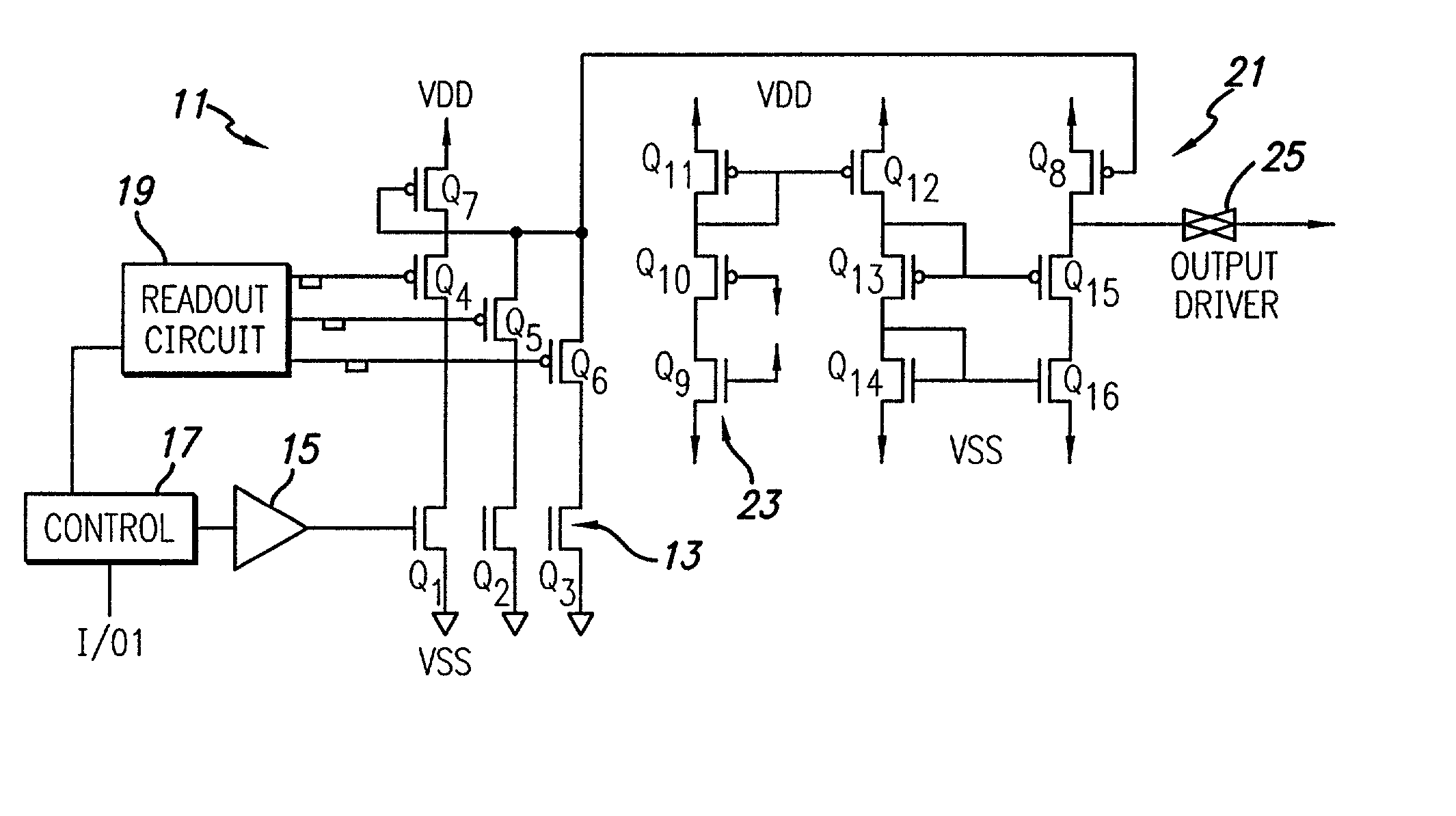
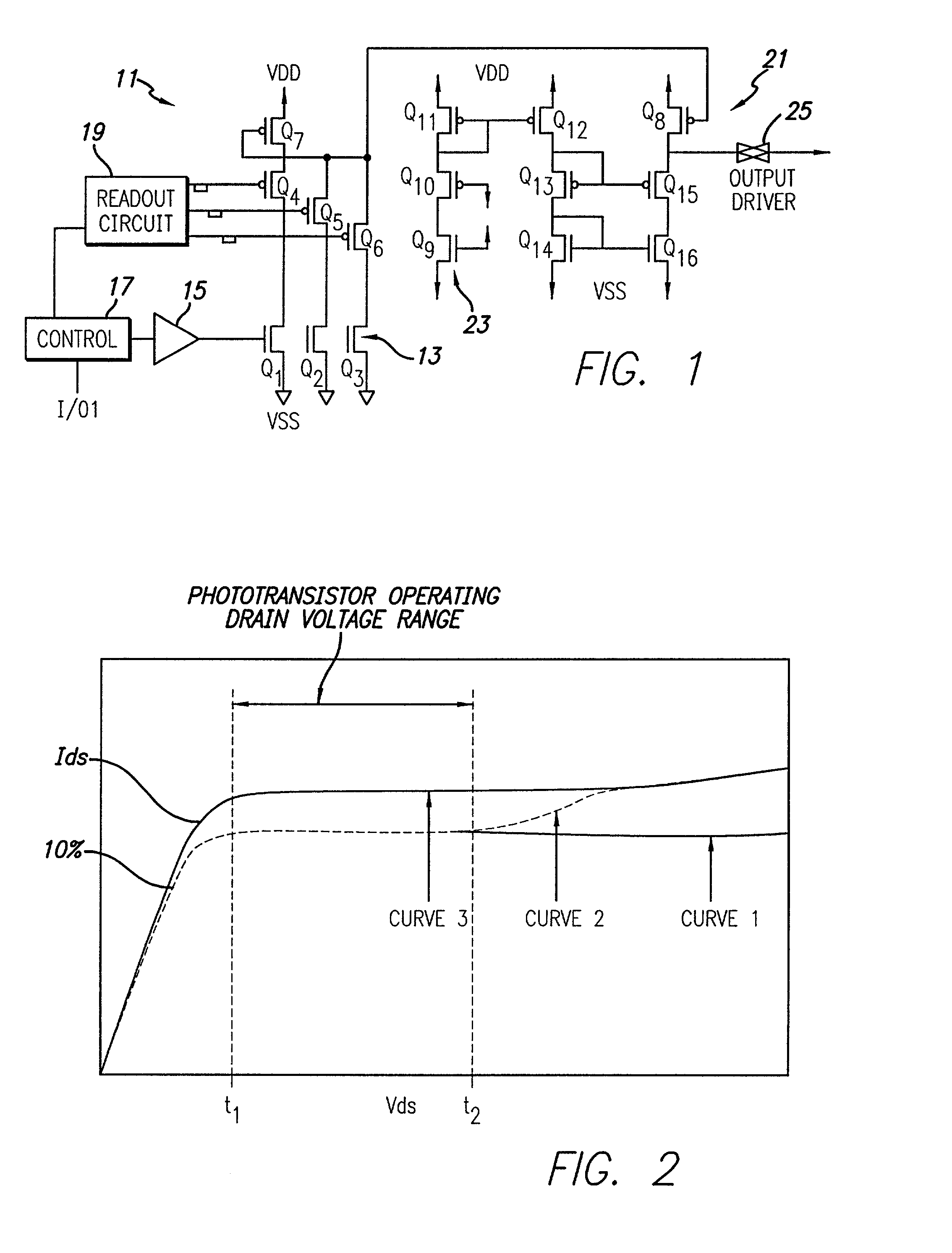
[0018] FIG. 1 is a schematic diagram of an illustrative implementation of a digital imaging system implemented in accordance with the teachings of the present invention. The inventive imager 11 includes an array 13 of detector elements of which a single row is shown with three transistors Q1, Q2 and Q3. Those skilled in the art will appreciate that...


PUM


Abstract

A detector with a transistor sensitive to electromagnetic energy. In accordance with the present teachings, the transistor is biased such that the output thereof is responsive to the electromagnetic energy. The inventive imager includes an array of the novel detectors. Each of the detectors being an n-channel metal-oxide semiconductor transistor with a floating body. The transistors are biased for selective activation and sequential readout. The transistor outputs are read by a differential current sense amplifier. A color filter is disclosed to provide a color sense capability. As an alternative, a grating is provided for this purpose. The present invention allows a very dense imager to be built on using conventional silicon on sapphire or silicon on insulator complementary metal-oxide semiconductor processes. The use of standard CMOS processes allows for low manufacturing costs.

Description

[0001] 1. Field of the Invention[0002] The present invention relates to imaging systems. More specifically, the present invention relates to digital imaging systems operative in the visible portion of the electromagnetic spectrum.[0003] 2. Description of the Related Art[0004] Imaging systems are well known in the art. These devices are used in cameras and detectors to provide an image of a scene or object for display or output purposes. Imaging systems are operative over various portions of the electromagnetic spectrum and at various intensity levels. For consumer, commercial, industrial and military applications, imaging systems operative in the visible portion of the electromagnetic spectrum are of particular utility.[0005] Existing imagers are typically implemented either with charge-coupled device (CCD) type technology or complementary metal-oxide semiconductor (CMOS) type technology. The CCD imager requires a high (e.g., 100%) yield of CCD elements. Accordingly, a high manufact...

Claims


Application Information

Patent Timeline
Patent Type & Authority Applications(United States)
IPC IPC(8): H01L27/146H01L31/0216H01L31/113H04N5/335
CPCH01L27/14621H01L27/14679H04N5/335H01L31/1136H04N3/155H01L31/02164H04N25/571H04N25/00
Inventor VU, TRUC Q.CALABRETTA, FRANKASBROCK, JAMES F.DO, NHAN T.
Owner RAYTHEON CO
Why Eureka
Try Eureka