Phase shift mask and design method therefor

a phase shift mask and design method technology, applied in the field of phase shift masks, can solve the problems of difficult to determine the width of the halftone region, difficult to know the optimal position, and difficult to use a photo mask to transfer and form a pattern having a size equal or less than the half of the exposure light wavelength in a conventional exposure method

Inactive Publication Date: 2002-11-28
NEC ELECTRONICS CORP
View PDF1 Cites 72 Cited by
  • Summary
  • Abstract
  • Description
  • Claims
  • Application Information

AI Technical Summary

Benefits of technology

[0021] Another object of the present invention is to provide a phase shift mask and the design method for it which can reduce time required for designing the "halftone region" and the "auxiliary pattern".
[0022] Another object of the present invention is to provide a phase shift mask and the design method for it which effectively restrain a deformation of a transferred pattern transferred on a wafer corresponding to an original pattern placed on the mask at a predetermined pitch.
[0023] Another object of the present invention is to provide a phase shift mask and the design method for it which surely provide a focal depth extension effect.

Problems solved by technology

Because the design rule has decreased to about a half of the wavelength of exposure light (an exposure wavelength) recently, it is extremely difficult to use a photo mask to transfer and form a pattern having a size equal to or less than the half of the exposure light wavelength on a resist film in a conventional exposure method.
Thus, there is such a problem as it takes a long time to determine the width of the halftone region.
When the placement pitch of the main pattern (the hole forming pattern) is small on the mask, the dimension of the transferred pattern on the wafer is fairly lager than a desired value, and there is such a problem as the neighboring transferred patterns may come in contact with each other.
There is such a problem as it is not easy to know the optimal position.

Method used


Image

  • Phase shift mask and design method therefor
  • Phase shift mask and design method therefor
  • Phase shift mask and design method therefor

Examples


first embodiment

[0076] (Constitution of Mask of First Embodiment)

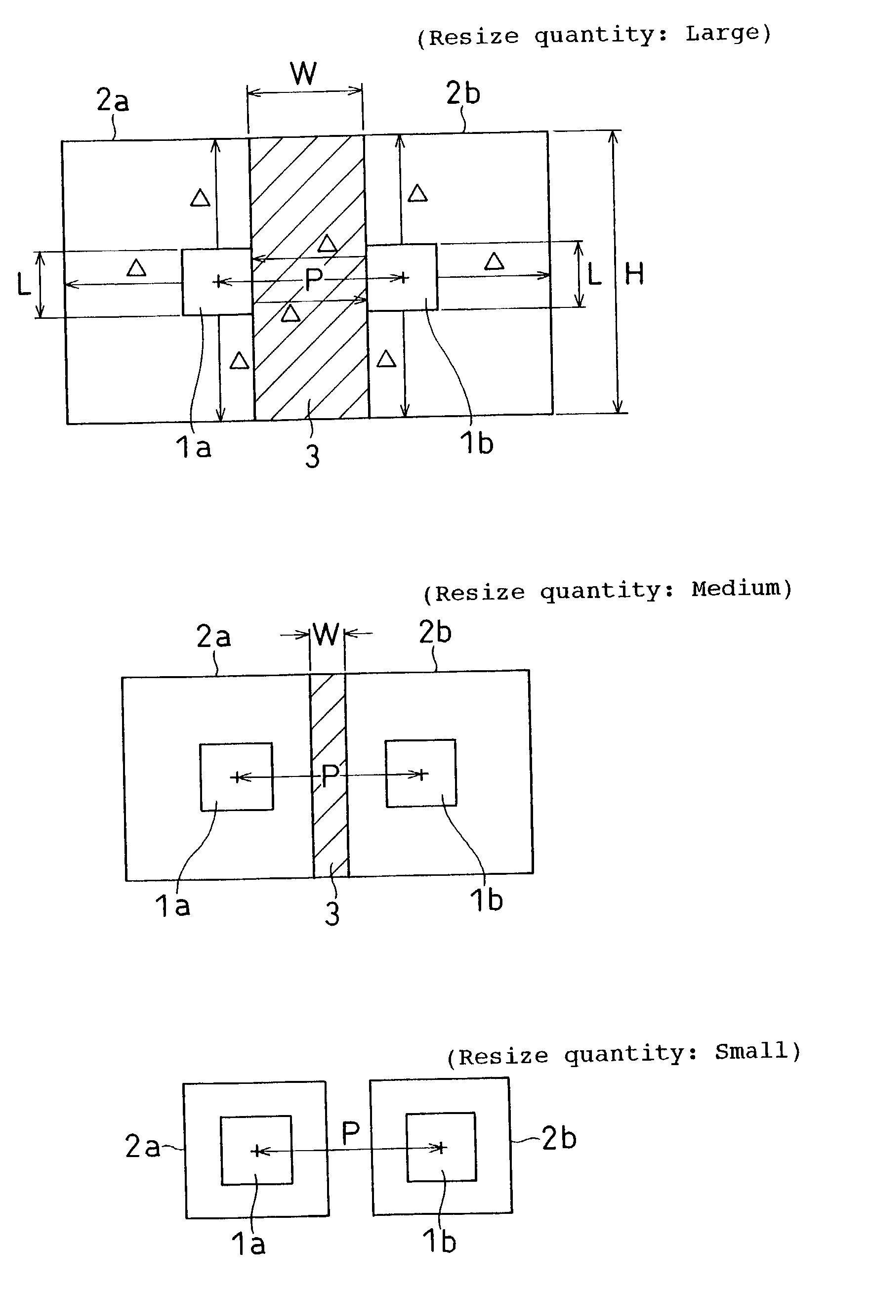
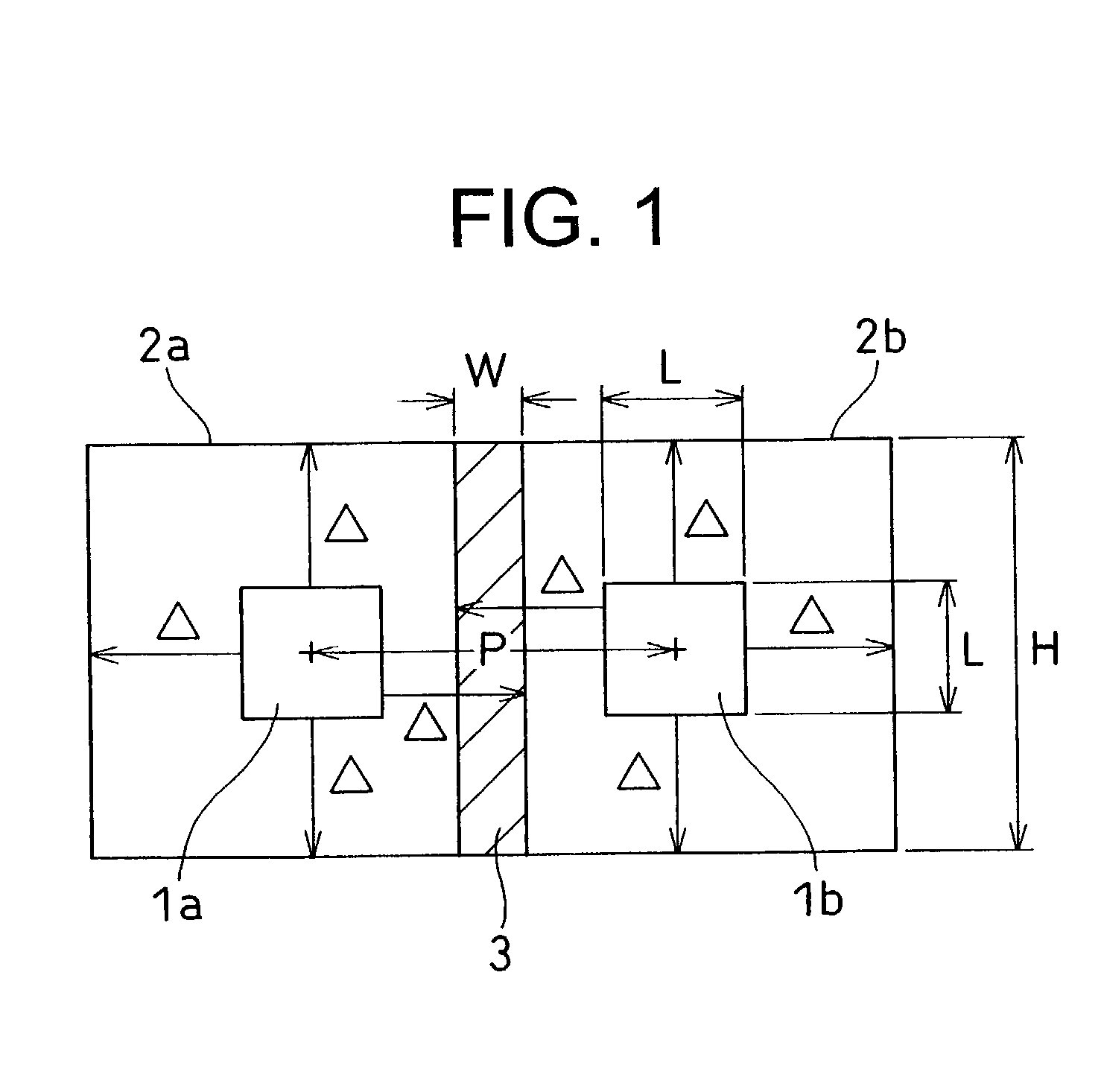
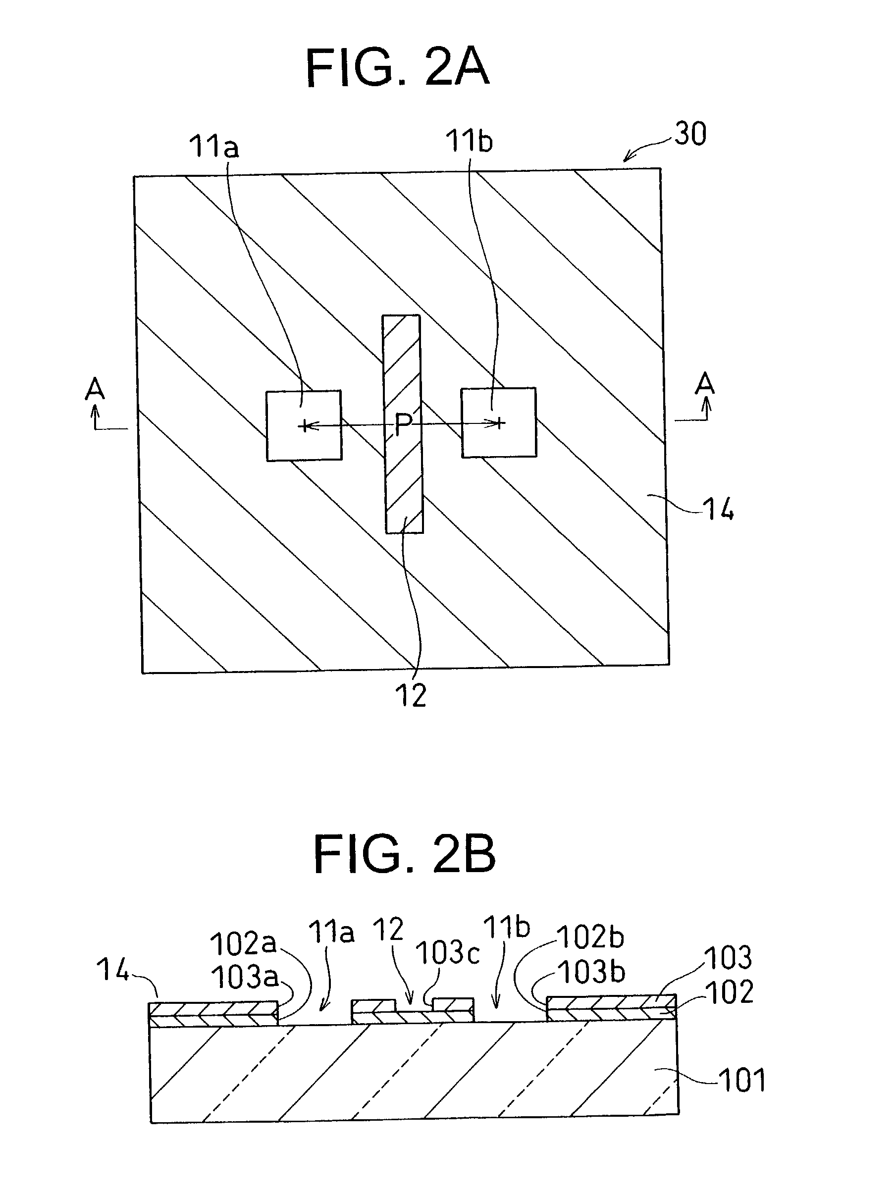
[0077] FIG. 1 is a conceptual drawing for showing a design method for a halftone type phase shift mask of a first embodiment of the present invention, and FIG. 2A and FIG. 2B are respectively a top view and a section view for showing the halftone type phase shift mask of the first embodiment of the present invention. This mask 10 is used to transfer and form two square hole forming patterns 1a and 1b placed with a pitch P as shown in FIG. 1 on a wafer. The patterns 1a and 1b have the same shape and dimension.

[0078] The halftone type phase shift mask 10 of the present invention has hole forming translucent regions 11a and 11b as the two squares placed with the pitch P, a halftone region 12 in a stripe shape (a long rectangle) placed between these translucent regions 11a and 11b, and a light shield region 14 covering around the translucent regions 11a and 11b, and the halftone region 12 on a transparent substrate 101 in FIG. 2A and FIG....

second embodiment

[0132] (Constitution of Mask of Second Embodiment)

[0133] FIGS. 7A and 7B are conceptual drawings for showing a design method for an auxiliary pattern type phase shift mask of a second embodiment of the present invention, and FIGS. 8A and 8B show a constitution of an auxiliary pattern type phase shift mask 30. This mask 30 is used to transfer and form one square hole forming pattern 21 as shown in FIGS. 7A and 7B on a wafer. While the mask 10 in the first embodiment is intended to increase the precision of the transferred hole dimension, the mask 30 of the second embodiment is intended to increase the focal depth.

[0134] The phase shift mask 30 of the present invention has one isolated square hole forming translucent region 31, an auxiliary pattern region 33 in a square ring shape placed to surround the translucent region 31, and a light shield region 34 for covering the outside of the auxiliary pattern 33 on a transparent substrate 111 in FIGS. 8A and 8B. The light shield region 34 i...

third embodiment

[0150] (Constitution of Mask of Third Embodiment)

[0151] FIGS. 9A and 9B show a halftone / auxiliary pattern type phase shift mask 40 of a third embodiment of the present invention. While the present invention is applied to the isolated hole forming pattern 21 in the mask 30 in FIGS. 7A and 7B, and FIGS. 8A and 8B, the present invention is applied to neighboring two hole forming patterns in the mask 40 of the present embodiment. The mask 40 corresponds to a combination of the first embodiment and the second embodiment.

[0152] The phase shift mask 40 has two square hole forming translucent regions 41a and 41b placed with a pitch of P, a halftone region 42 in a stripe shape (a long rectangle) placed between these translucent regions 41a and 41b, an auxiliary pattern region 43 in a rectangular ring shape placed around these translucent regions 41a and 41b, and the halftone region 42, and a light shield region 44 for covering the outside of the auxiliary pattern region 43 on a transparent s...


PUM

PropertyMeasurementUnit
exposure wavelengthaaaaaaaaaa
wavelengthaaaaaaaaaa
widthaaaaaaaaaa

Abstract

After a plurality of main patterns are placed at a predetermined pitch P, the individual main patterns are extended by a predetermined resize quantity DELTA to form virtual regions. When the virtual regions have an overlapped part, the overlapped part is placed between the virtual regions, and is set as a halftone region forming part having a predetermined transmission factor T with respect to exposure light. The resize quantity DELTA and the transmission factor T are set such that a transferred size of the main patterns on a predetermined resist film is settled within a desired range according to the change of the pitch P under a predetermined exposure condition.

Description

[0001] 1. Technical Field of the Invention[0002] The present invention relates to a phase shift mask used in a lithography process as one manufacturing process for a semiconductor integrated circuit device (LSI), and specifically relates to a phase shift mask including a halftone region, an auxiliary pattern region, or both of them, and a design method of the phase shift mask.[0003] 2. Description of the Related Art[0004] As the operation speed and the integration of semiconductor devices have been increasing in the LSI recently, it is required to miniaturize different types of patterns on layers constituting the semiconductor devices. Because the design rule has decreased to about a half of the wavelength of exposure light (an exposure wavelength) recently, it is extremely difficult to use a photo mask to transfer and form a pattern having a size equal to or less than the half of the exposure light wavelength on a resist film in a conventional exposure method. Different methods hav...

Claims


Application Information

Patent Timeline
Patent Type & Authority Applications(United States)
IPC IPC(8): G03F1/29G03F1/32G03F1/36G03F1/68H01L21/027
CPCG03F1/36G03F1/32H01L21/027
Inventor TANAKA, SATSUKI
Owner NEC ELECTRONICS CORP
Why Eureka
Try Eureka