Structuring method

a structure method and structure technology, applied in the field of structure methods, can solve the problems of reducing resolution, difficult for further photolithographic processing of wafers, and affecting the quality of metal films deposited in the deposition step following the exposure,

Inactive Publication Date: 2003-01-30
HEWLETT PACKARD DEV CO LP
View PDF4 Cites 9 Cited by
  • Summary
  • Abstract
  • Description
  • Claims
  • Application Information

AI Technical Summary

Problems solved by technology

Due to the nonplanar surface of the semi-processed wafer, a further photolithographic processing of the wafer is difficult.
Therefore, a metal film deposited in a deposition step follo

Method used


Image

  • Structuring method
  • Structuring method
  • Structuring method

Examples


Embodiment Construction

[0029] In the following a detailed description of preferred embodiments of the invention will be given, referring to the drawings.

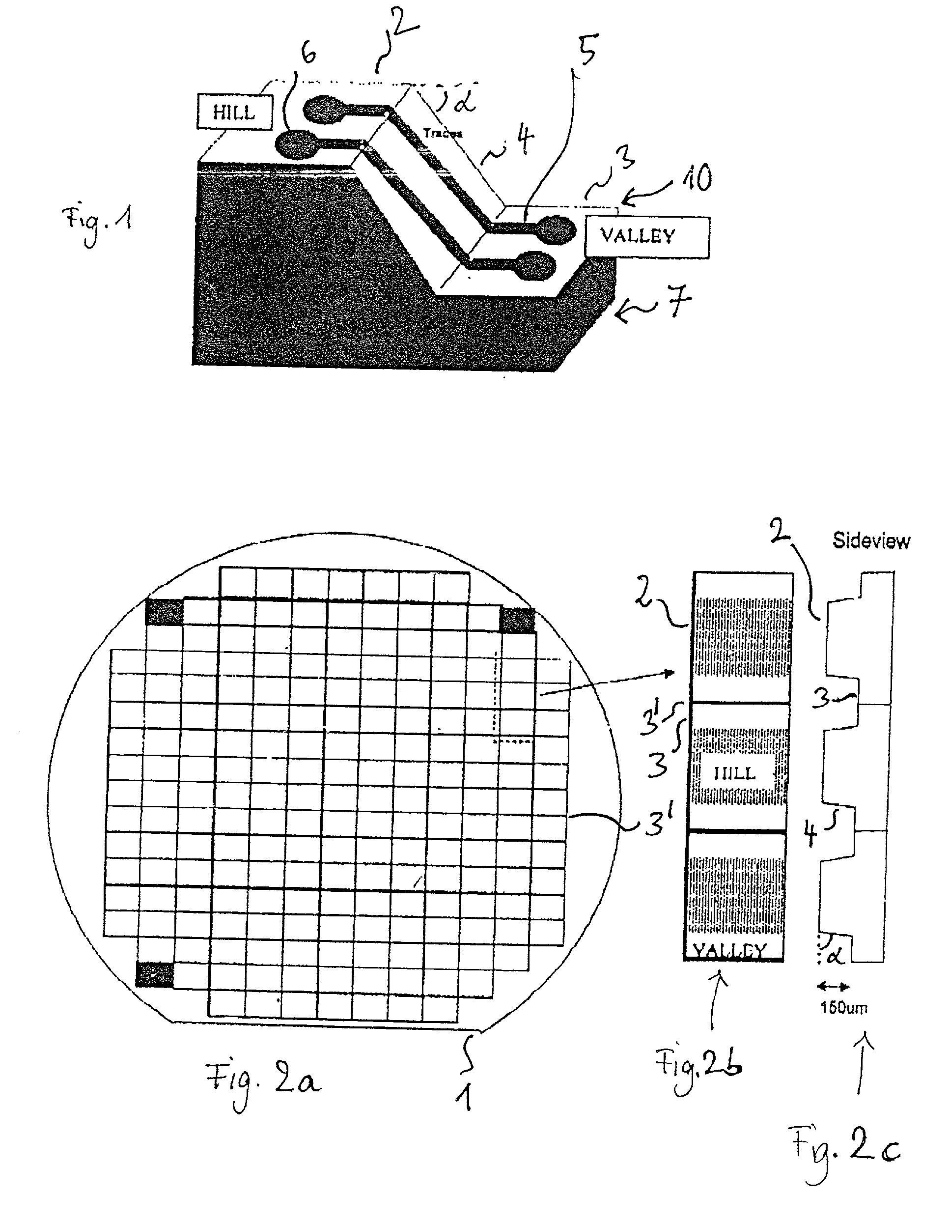
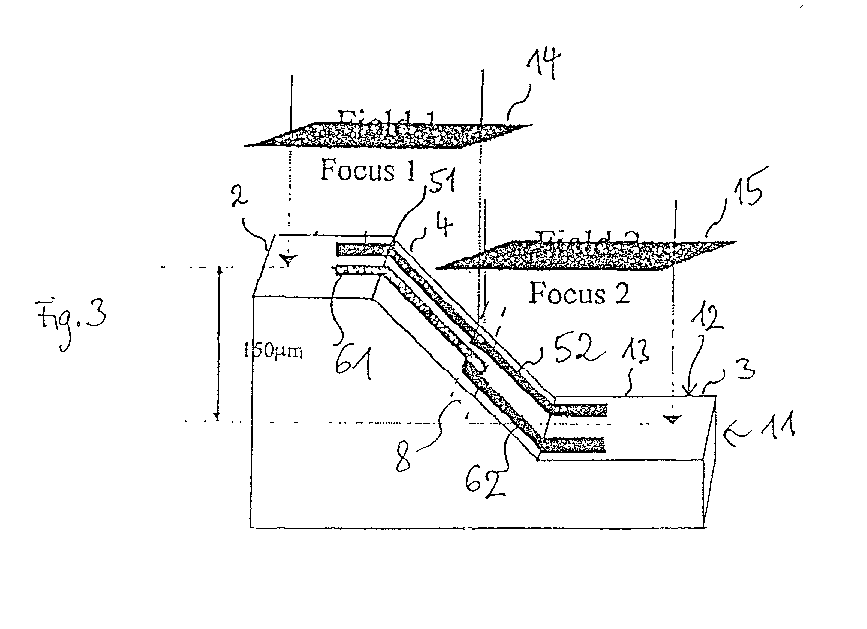
[0030] FIG. 1 shows a perspective partial view of a die 7 having a processed nonplanar surface 10, according to a preferred embodiment of the present invention. The surface 10 comprises a single step structure. The surface 10 is thus nonplanar, i.e. comprises different regions not all extending in a single plane. The single step structure comprises a plane top face 2 extending in a first plane, and a plane bottom face 3 extending in a second plane, which extends, in the view of FIG. 1, at a lower level than the first plane. The top face 2 and the bottom face 3 are interconnected by a sloping step face 4. The sloping step face 4 is sloping from the top face 2 toward the bottom face 3 at an angle .alpha. of about 60.degree..

[0031] The processed surface 10 further comprises two elongated conductive structures 5 and 6 extending continuously from the top face ...


PUM


Abstract

The invention provides a structuring method, in particular for stepped wafer or die surfaces. The method includes photolithographically exposing a pattern comprising at least a first pattern portion and a second pattern portion onto a surface, said surface comprising at least a first surface portion at which a tangential plane to the surface extends in a first plane and a second surface portion at which a tangential plane to the surface extends in a second plane not coinciding with the first plane. The method comprises a first exposure step, in which the first pattern portion is exposed. Therein, the first pattern portion is focused into a first focal plane. The method further comprises a second exposure step, in which the second pattern portion is exposed. Therein, the second pattern portion is focused into a second focal plane which is different from the first focal plane.

Description

[0001] 1. Field of the Invention[0002] The invention relates to a structuring method including photolithographic exposure of a pattern onto a nonplanar surface being structured perpendicular to the surface and a die which has been fabricated using the structuring method.[0003] 2. Related Art[0004] The fabrication of high topography semiconductor devices from a wafer includes a great number of processing steps, such as photolithography and material deposition or application steps. After a number of processing steps have been performed to generate a semi-processed wafer, the originally planar wafer surface usually has become highly nonplanar. For example, the surface of the semi-processed wafer comprises a structure of plateau-like planar regions at different levels and sloping step regions connecting the different plateau-like planar regions.[0005] An example for a nonplanar semi-processed wafer is a stepped wafer which has a surface having an array of parallel trenches. Each trench ...

Claims


Application Information

Patent Timeline
IPC IPC(8): G03F7/20G03F7/207H01L21/027
CPCG03F7/703
Inventor ARIFIN, JULIANATRAN, THINH VAN
Owner HEWLETT PACKARD DEV CO LP
Why Eureka
Try Eureka