Redundancy circuit and method for flash memory devices

Inactive Publication Date: 2003-02-06
MICRON TECH INC
View PDF0 Cites 1 Cited by
  • Summary
  • Abstract
  • Description
  • Claims
  • Application Information

AI Technical Summary

Problems solved by technology

This results in a relatively small silicon area and the effectuation of large scale integration.
The tradeoff here is that a larger surface area of silicon is required and therefore a smaller scale of integration is achieved.
However, the ability of the existing flash memory device of FIG. 1 to replace defective columns of memory cells is limited as the number of defective columns increases.

Method used


Image

  • Redundancy circuit and method for flash memory devices
  • Redundancy circuit and method for flash memory devices
  • Redundancy circuit and method for flash memory devices

Examples


Embodiment Construction

[0019] The present invention will now be described more fully hereinafter with reference to the accompanying drawings in which an exemplary embodiment of the invention is shown. This invention may, however, be embodied in many different forms and should not be construed as being limited to the embodiment set forth herein. Rather, the embodiment is provided so that this disclosure will be thorough and complete, and will fully convey the scope of the invention to those skilled in the art.

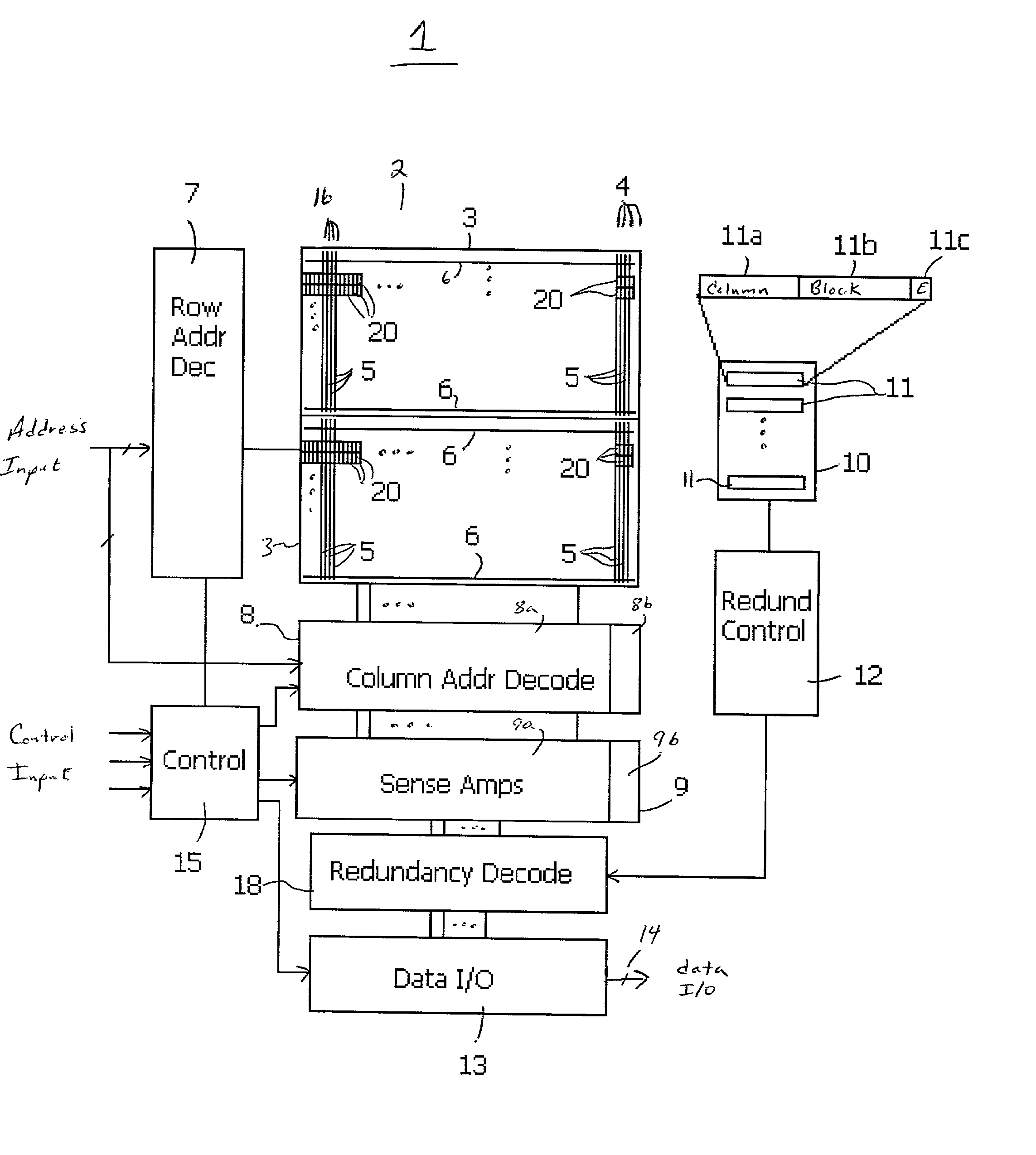
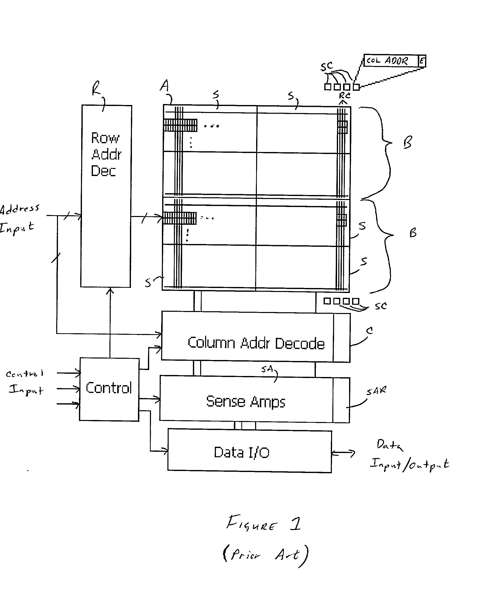
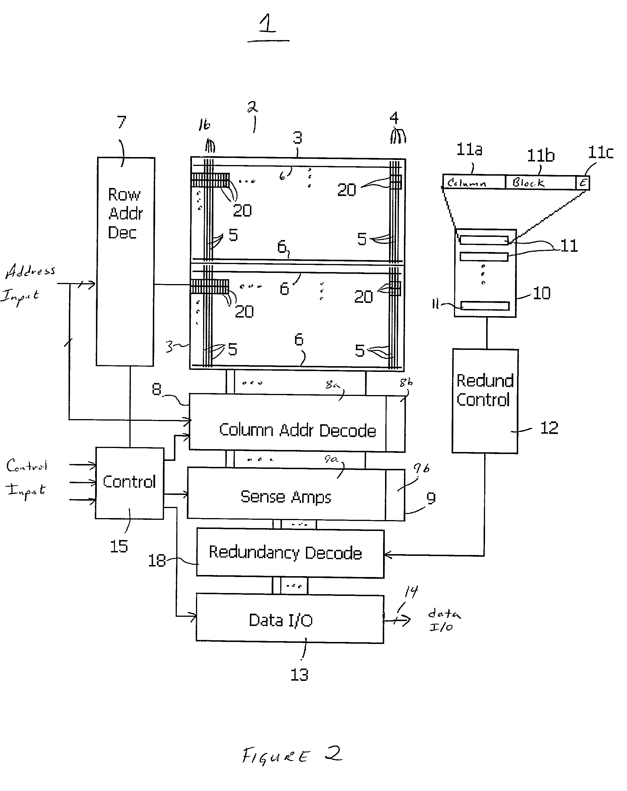
[0020] Referring to FIG. 2, there is shown a nonvolatile memory device 1 according to an exemplary embodiment of the present invention. Although it is understood that the nonvolatile memory device 1 may be virtually any type of nonvolatile memory device, nonvolatile memory device 1 will be described below as a flash memory device for reasons of simplicity.

[0021] In general terms, flash memory device 1 includes redundant circuitry for efficiently replacing columns of memory cells 20 having a defect. Fl...


PUM


Abstract

A method and circuit are disclosed for replacing defective columns of flash memory cells in a flash memory device. The circuit includes a plurality of sets of storage elements, each set of storage elements being capable of identifying at least one column of memory cells in any block of memory cells as being defective. The circuit further includes control circuitry for replacing an addressed column of memory cells with a redundant column of memory cells upon an affirmative determination that a set of storage elements identifies the addressed column of memory cells as being defective.

Description

[0001] 1. Technical Field of the Invention[0002] The present invention relates to nonvolatile memory devices, and particularly to nonvolatile memory devices having column redundancy.[0003] 2. Description of the Related Art[0004] The first nonvolatile memories were electrically programmable read-only memories (EPROMs). In these memories, the memory cells include a floating-gate transistor that is programmable using the hot carrier effect. Programming of an EPROM memory cell includes applying a potential difference between the drain and the source of the floating gate transistor in the presence of a high potential difference (of about 20 volts, this value varying according to the desired programming speed) between the control gate and the source. The application of the first of these potential differences generates an electrical field that gives rise to a flow of electrons in the channel. These electrons collide with atoms of the channel, causing the appearance of new free electrons. ...

Claims


Application Information

Patent Timeline
IPC IPC(8): G11C16/06G11C29/00G11C29/04
CPCG11C29/808G11C29/81
Inventor MATARRESE, STELLAFASOLI, LUCA GIOVANNI
Owner MICRON TECH INC
Why Eureka
Try Eureka