
Mos-gated power semiconductor device

a technology of metal oxide semiconductors and power semiconductors, applied in the direction of semiconductor devices, electrical appliances, transistors, etc., can solve the problems of reducing the switching speed of the device, and achieve the effects of reducing on-resistance, reducing breakdown voltage, and not increasing parasitic capacitan

Inactive Publication Date: 2003-03-27
FAIRCHILD KOREA SEMICON
View PDF0 Cites 61 Cited by
  • Summary
  • Abstract
  • Description
  • Claims
  • Application Information

AI Technical Summary

Benefits of technology

0009] The invention includes a MOS-gated power semiconductor device in which breakdown voltage is not reduced, the parasitic capacitance is not increased, and the On-resistance is reduced.

Problems solved by technology

Further, parasitic capacitance components can be increased when implementing this suggestion, thereby reducing the switching speed of the device.

Method used


Image

  • Mos-gated power semiconductor device
  • Mos-gated power semiconductor device
  • Mos-gated power semiconductor device

Examples


Embodiment Construction

[0025] The invention now will be described more fully with reference to the accompanying drawings, in which preferred aspects of the invention are shown. This invention may, however, be embodied in many different forms and should not be construed as being limited to the aspects set forth herein. Rather, these aspects are provided so that this disclosure will be thorough and complete, and will fully convey the concept of the invention to those skilled in the art. In the drawings, the thickness of layers and regions are exaggerated for clarity. It will also be understood that when a layer is referred to as being "on" another layer or substrate, it can be directly on the other layer or substrate, or intervening layers may also be present. The same reference numerals in different drawings represent the same element, and thus their description will be omitted.

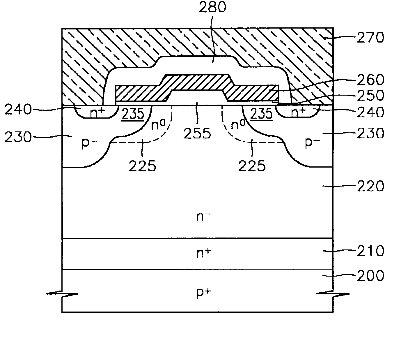
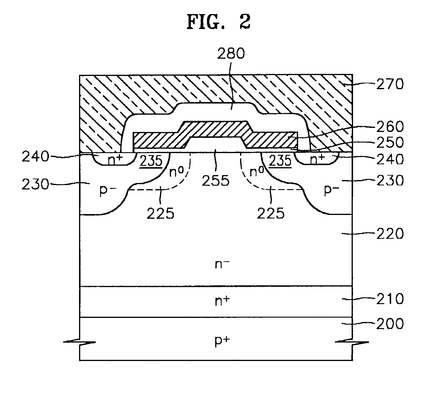
[0026] FIG. 2 is a cross-sectional view of MOS-gated power semiconductor device in one aspect of the invention. In this aspect of ...


PUM


Abstract

A MOS-gated power semiconductor device is described. The MOS-gated power semiconductor device includes a semiconductor substrate that is heavily doped with impurities of a first conductivity type and used as a collector region, a drift region lightly doped with impurities of a second conductivity type on the substrate, a gate insulating layer on the drift region having a center thicker than its edges, a gate electrode on the gate insulating layer, a well region that is lightly doped with impurities of a first conductivity type on the drift region and that has a channel region overlapping a portion of the gate electrode, an emitter region that is heavily doped with impurities of a second conductivity type and that contacts the channel region, an emitter electrode electrically connected to the emitter region and isolated from the gate electrode, and a collector electrode electrically connected to the semiconductor substrate.

Description

[0001] FIELD OF THE INVENTION[0002] The invention generally relates to methods for fabricating integrated circuits (ICs) and semiconductor devices and the resulting structures. More particularly, the invention relates to metal oxide semiconductor (MOS) gated power semiconductor devices and methods for making such devices.[0003] BACKGROUND OF THE INVENTION[0004] FIG. 1 depicts a cross-sectional view of an insulated gate bipolar transistor (IGBT), which is one type of a conventional MOS-gated power semiconductor device. As depicted in FIG. 1, a p+ type semiconductor substrate 100 is used as a collector region. On the p+ type semiconductor substrate 100 are sequentially located an n+ type buffer layer 110 and an n- type drift region 120. A p- type well region 130 is located on the n-type drift region 120. As well, n+ type emitter regions 140 are located on the p- type well region 130.[0005] Still referring to FIG. 1, a gate electrode 160 with a gate insulating layer 150 at its bottom i...

Claims


Application Information

Patent Timeline
Patent Type & Authority Applications(United States)
IPC IPC(8): H01L21/334H01L21/331H01L29/08H01L29/423H01L29/739H01L29/78
CPCH01L29/0847H01L29/42368H01L29/66333H01L29/7395H01L29/7802H01L29/0878H01L21/18
Inventor YUN, CHONG-MANKIM, SOO-SEONGLEE, KYU-HYUNKIM, YOUNG-CHULL
Owner FAIRCHILD KOREA SEMICON
Features
  • Generate Ideas
  • Intellectual Property
  • Life Sciences
  • Materials
  • Tech Scout
  • Unparalleled Data Quality
  • Higher Quality Content
  • 60% Fewer Hallucinations
Learn More