Input/output circuit, reference-voltage generating circuit, and semiconductor integrated circuit

a reference-voltage generating circuit and input/output circuit technology, applied in the direction of transmission, transmission line coupling arrangement, amplifier input/output impedence modification, etc., can solve the problem of timing error such as clock duty error and clock skew, and the reference voltage from the reference-voltage source is not compatible with the logical threshold valu

Inactive Publication Date: 2003-05-01
LONGITUDE LICENSING LTD
View PDF4 Cites 63 Cited by
  • Summary
  • Abstract
  • Description
  • Claims
  • Application Information

AI Technical Summary

Benefits of technology

0034] FIG. 9 is a diagram illustrating an example of

Problems solved by technology

Further, in the conventional circuit, the transmitted signal in the output circuit is reflected again owing to mismatch of impedance with respect to the signal source of the line.
However, in the conventional circuit in which the reference voltage is supplied from a reference-voltage source exterior to the chip, a mismatch occurs between the reference voltage from the reference

Method used


Image

  • Input/output circuit, reference-voltage generating circuit, and semiconductor integrated circuit
  • Input/output circuit, reference-voltage generating circuit, and semiconductor integrated circuit
  • Input/output circuit, reference-voltage generating circuit, and semiconductor integrated circuit

Examples


first embodiment

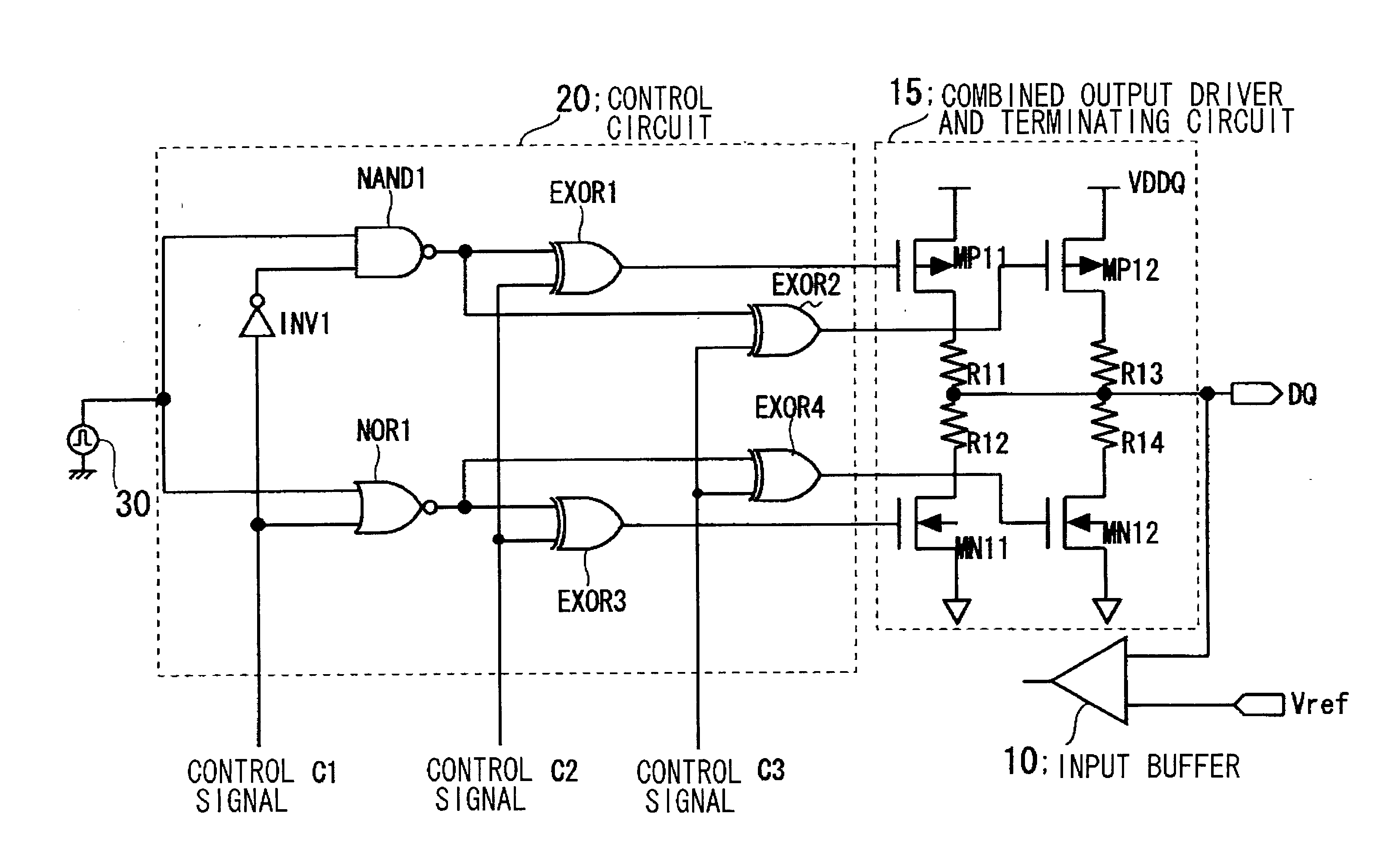
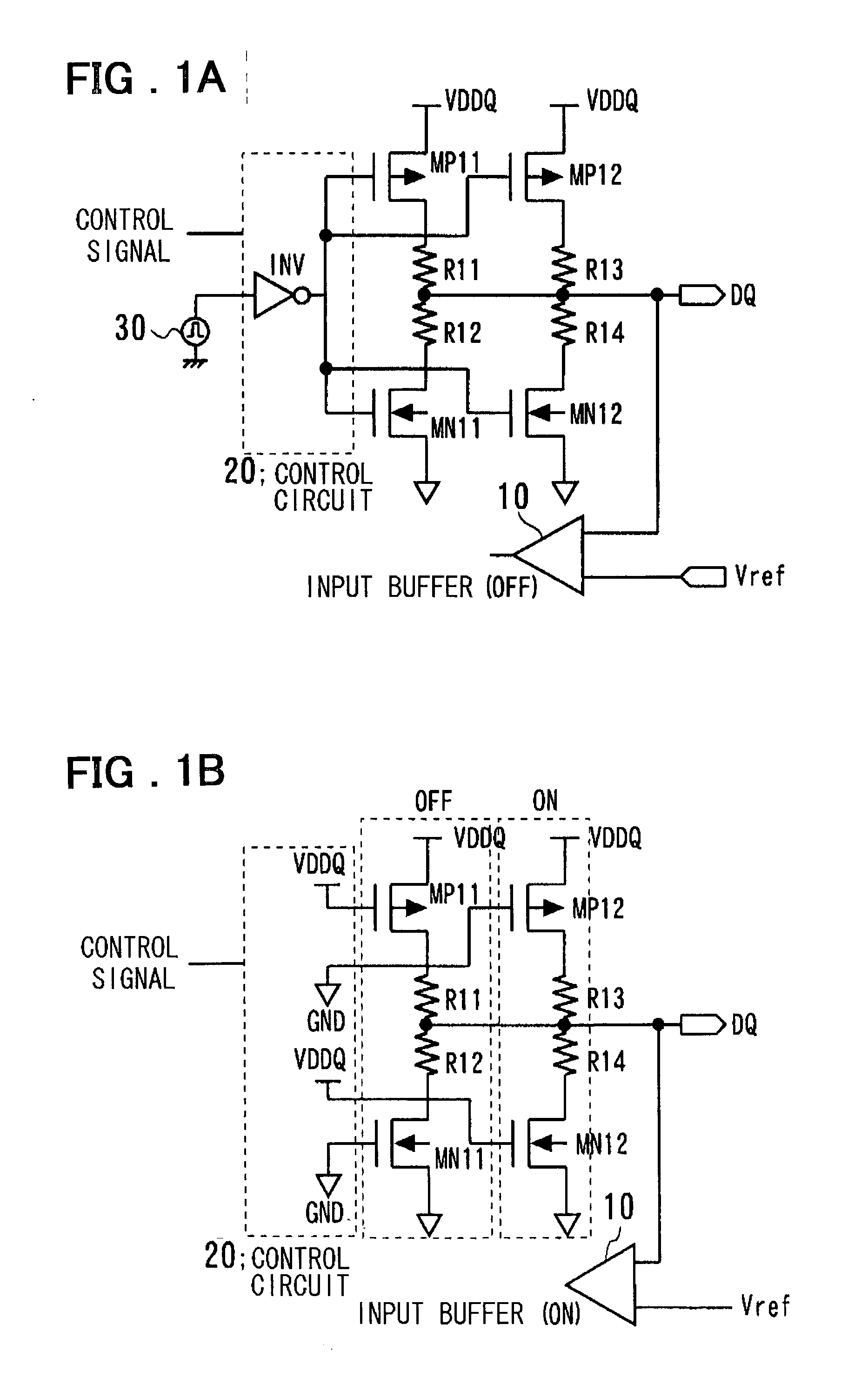
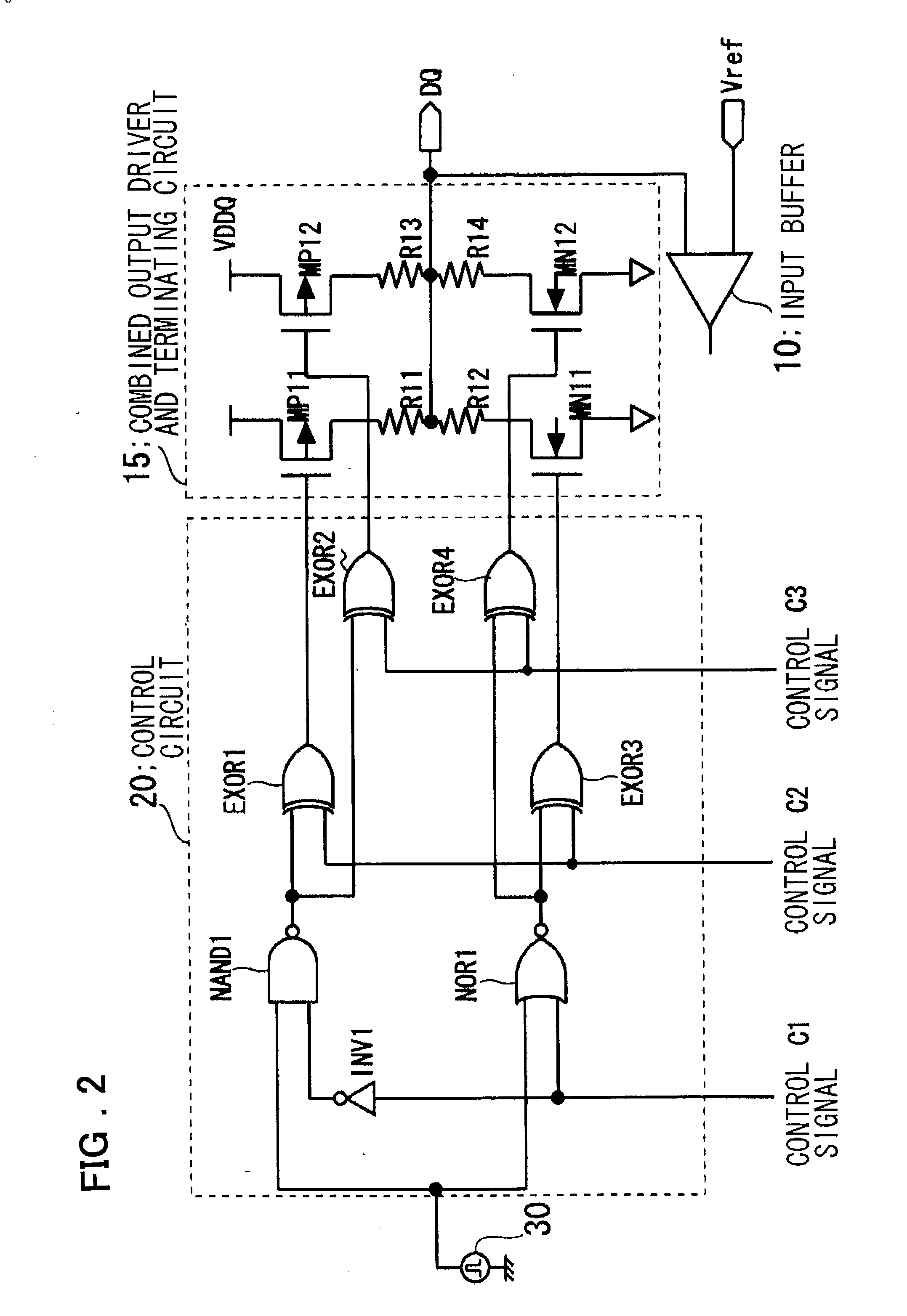
[0044] FIGS. 1A and 1B are circuit diagrams useful in describing the present invention, in which FIG. 1A illustrates the circuit connections at the time of signal transmission from the input / output circuit (i.e., in the output mode) and FIG. 1B the circuit connections at the time of signal reception (i.e., in the input mode). The output and input modes are decided by a command from a host device (not shown), and a control signal for controlling input / output is set to a logical value that is in accordance with the output or input mode. The method of generating the control signal is not directly related to the gist of the present invention and need not be described.

[0045] Referring to FIG. 1A, data from a data source 30 and a control signal for controlling input / output are supplied to a control circuit 20. When the control signal is indicative of the output mode, the control circuit 20 outputs a signal obtained on inverting the data by an inverter INV. The input / output circuit include...

third embodiment

[0077] FIG. 5 illustrates the structure of the present invention. This illustrates another structure of a circuit for generating the reference voltage Vref. As shown in FIG. 5, the circuit for generating the reference voltage Vref according to the present embodiment has an operational amplifier 41 that functions as a voltage follower. The operational amplifier 41 has a non-inverting input terminal (+) which is connected to the connection node of resistors R41 and R42, and an output terminal which is connected to its inverting input terminal (-). The output voltage of this voltage follower is supplied to the input buffer 10 as the reference voltage Vref. By virtue of this arrangement, the voltage follower exercises control in such a manner that the output voltage thereof is held equal to the reference voltage applied to the non-inverting input terminal (+), regardless of the effects of noise or the like, and thus the reference voltage supplied to the input buffer 10 is held fixed.

fourth embodiment

[0078] FIG. 6 illustrates the structure of the present invention and shows another structure of a circuit for generating the reference voltage Vref. As shown in FIG. 6, the voltage at the connection node between the resistors R41 and R42 of the reference-voltage generating circuit 40 is supplied to the input buffer 10 as the reference voltage Vref, and the connection node between the between the resistors R41 and R42 is connected to an external terminal (pin) Vref. The latter is connected to a dummy output circuit 60 of another chip by wiring (DQ dummy wiring). Since the dummy output circuit 60 of the other chip functions as a circuit for generating the reference voltage, it is illustrated as reference-voltage generating circuit 60. The dummy output circuit (reference-voltage generating circuit) 60 comprises a CMOS inverter whose input and output nodes are connected together. More specifically, the reference-voltage generating circuit 60 includes a P-channel MOS transistor MP61 whos...


PUM


Abstract

Disclosed is an input/output circuit having a terminating circuit that contributes to a smaller chip area. The input/output includes an output buffer having a first series circuit, which comprises a first transistor and a resistor and a second series circuit, which comprises a second transistor and a resistor, connected in parallel between a high-potential power supply and an input/output pin, as well as a third series circuit, which comprises a third transistor and a resistor and a fourth series circuit, which comprises a fourth transistor and a resistor, connected in parallel between the input/output pin and a low-potential power supply. The input/output circuit further includes an input buffer having an input terminal connected to the input/output pin, and a control circuit which, at the time of a signal output, performs control for supplying a signal, which is obtained by inverting the logic of output data, to gates of the first to fourth transistors, and which, at the time of a signal input, performs control for supplying the gates of the first and third transistors with the high-potential power supply voltage and low-potential power supply voltage, respectively, and the gates of the second and fourth transistors with the low-potential power supply voltage and high-potential power supply voltage, respectively.

Description

[0001] This invention relates to a bi-directional input / output interface for a signal input and output and, more particularly, to a termination of a transmission line and to a reference-voltage generating circuit.[0002] In a high-speed logic circuit in which signal rise and fall times are short, there are instances where it becomes necessary to treat a signal line as a transmission line of a distributed-constant circuit. For example, reflection must be taken into account when the propagation delay time of a transmission line is large in comparison with the rise and fall times of the output signal. That is, when a circuit having impedance different from the characteristic impedance of a transmission line is connected to the transmission line, reflection is produced at the point of connection. As is well known, a reflection coefficient .rho.1 at the receiving end is given by the following equation:.rho.1=(ZL-Z0) / (ZL+Z0)[0003] where Z0 represents the characteristic impedance of the lin...

Claims


Application Information

Patent Timeline
IPC IPC(8): H03K19/0175H03F1/56H03F3/62H03K19/0185H04L25/02
CPCH03K19/018592H04L25/0292H04L25/028H04L25/0278H03K19/0175
Inventor FUNABA, SEIJI
Owner LONGITUDE LICENSING LTD
Why Eureka
Try Eureka