
Test handler

a handler and handle technology, applied in the field of handlers, can solve the problems of inefficient size of handlers, long indexing time of test tray 70, and inability to load lots of user tray

Inactive Publication Date: 2003-05-08
TECHWING CO LTD
View PDF0 Cites 44 Cited by
  • Summary
  • Abstract
  • Description
  • Claims
  • Application Information

AI Technical Summary

Problems solved by technology

Therefore, it has disadvantage in that the indexing time of the test tray 70 is long and the amount of the devices in a unit time are not so many.
Therefore, it has another disadvantage that the size of the handler becomes larger inefficiently.
Additionally, the space for another components, for example, the user tray supplier 10 or the user tray deliver 20, is so limited that lots of the user tray can not be loaded.
Therefore, the size of the lot in an operation is limited so that the equipment operation ratio is declined.

Method used


Image

  • Test handler
  • Test handler
  • Test handler

Examples


Embodiment Construction

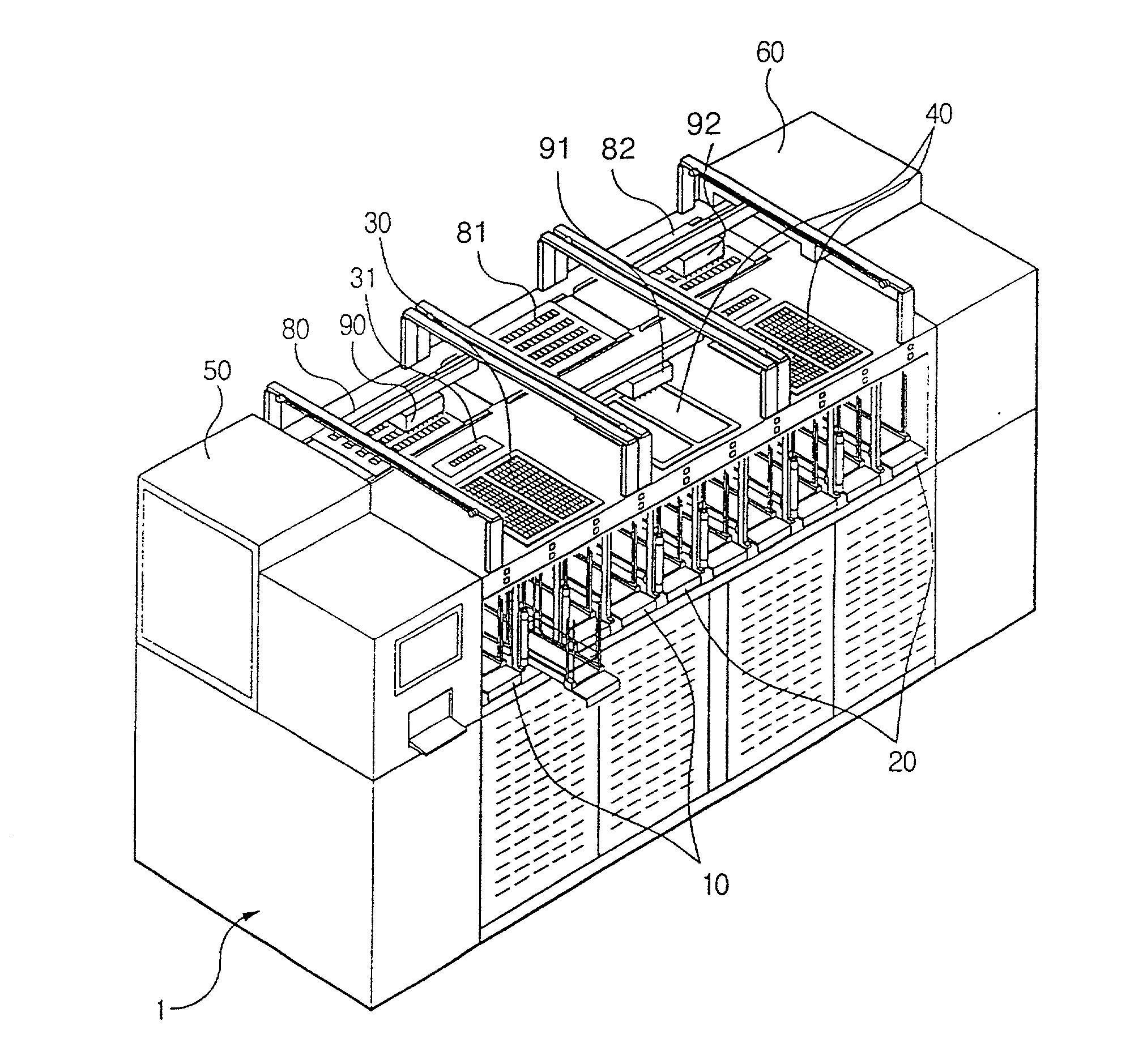
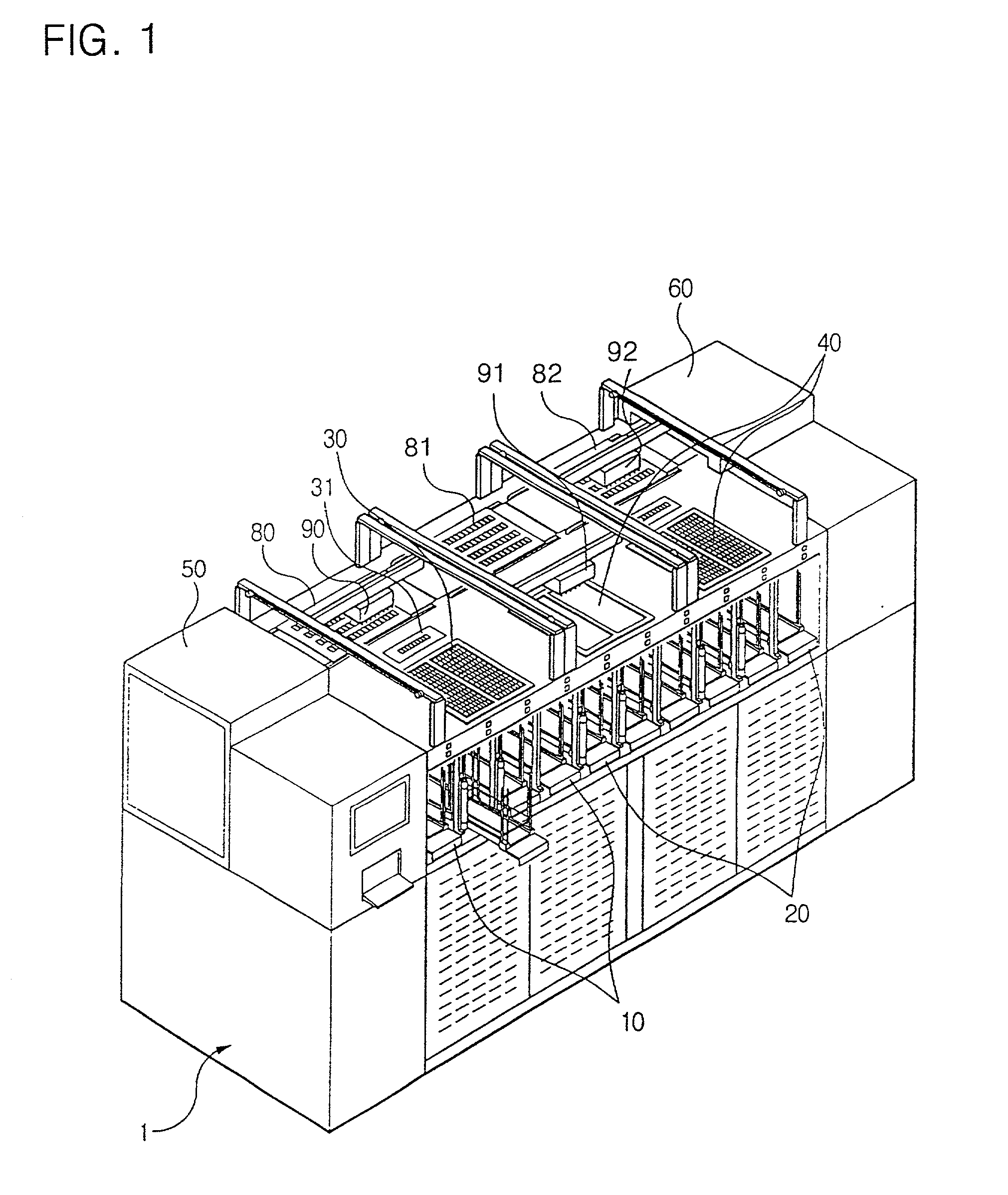
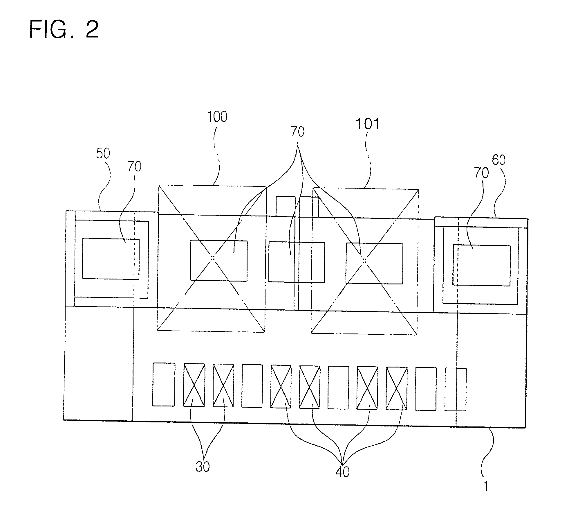
[0057] To accomplish the above described objects, the present invention provides a test handler for transferring more than one semiconductor device to connect to a test head for testing the semiconductor device and for classifying the semiconductor device according to the test results. The test handler comprises a main body, a stocker, a plurality of test trays, a device loading means, a first tray inverter, a soak chamber, a test chamber, a de-soak chamber, a second tray inverter, and a device unloading means. The stocker, prepared within the main body, includes a user tray supplier for loading plurality of user trays supplying a predetermined amount of the semiconductor devices for a test and a user tray deliver loading plurality of user trays carrying the classified semiconductor device according to the test results. The plurality of test trays are arranged according to the moving direction for testing the semiconductor device. The device loading means transfers the semiconductor...


PUM


Abstract

The present invention discloses a test handler comprising a main body, a stocker including a user tray supplier and a user tray deliver for loading plurality of user trays carrying the semiconductor device during devices tests, a plurality of test trays, a device loading means for transferring the devices in the user tray of the user tray supplier to the test tray, a first tray inverter changing the horizontal posture of the test tray, a soak chamber preparing a desired test temperature condition, a test chamber accomplishing tests, a de-soak chamber restoring the devices temperature, a second tray inverter inverting to the test tray of a horizontal posture, a device unloading means transferring the semiconductor devices on the test tray. The present invention can double the lot size in unit operation to improve equipment operation ratio. In more, the device loading time and unloading can be reduced so that the number of the devices treated in unit operation can be increased.

Description

[0001] 1. Field of the Invention[0002] The present invention is related to a test handler, and more particularly, to a test handler for testing an electric component (in this application, a `device` is designated for an electric component in the following statements) such as an integrated circuit (IC) or a semiconductor chip.[0003] 2. Description of the Related Art[0004] The device manufactured through a predetermined assembly process in a semiconductor manufacturing process, should perform a test process for checking whether a predetermined function in the device is operated or not. A test handler is employed in such a test process, and the test process is accomplished by transferring a predetermined number of the devices and by contacting a test head to the devices. According to the test results, the devices are classified and transferred.[0005] Such a test handler transfers the 32 or 64 devices to the test head for testing simultaneously, and performs a test in the abnormal tempe...

Claims


Application Information

Patent Timeline
IPC IPC(8): G01R31/28H01L21/00H01L21/677
CPCG01R31/2887G01R31/2893H01L21/67778H01L21/67242H01L21/67236
Inventor SHIM, JAE-GYUNJEON, SEUNG-WONNA, YUN-SUNGJEON, IN-GU
Owner TECHWING CO LTD
Learn More