Method and apparatus for producing bonded dielectric separation wafer

a technology of dielectric separation and bonded wafers, applied in electrical equipment, basic electric elements, semiconductor devices, etc., can solve the problems of silicon wafers being prone to breakage, unable to completely remove the process, and unable to bond the supporting substra

a technology of dielectric separation and bonded wafers, applied in electrical equipment, basic electric elements, semiconductor devices, etc., can solve the problems of silicon wafers being prone to breakage, unable to completely remove the process, and unable to bond the supporting substra

US20030092244A1Inactive Publication Date: 2003-05-15SUMITOMO MITSUBISHI SILICON CORP

Image

  • Method and apparatus for producing bonded dielectric separation wafer
  • Method and apparatus for producing bonded dielectric separation wafer
  • Method and apparatus for producing bonded dielectric separation wafer

Examples


Embodiment Construction

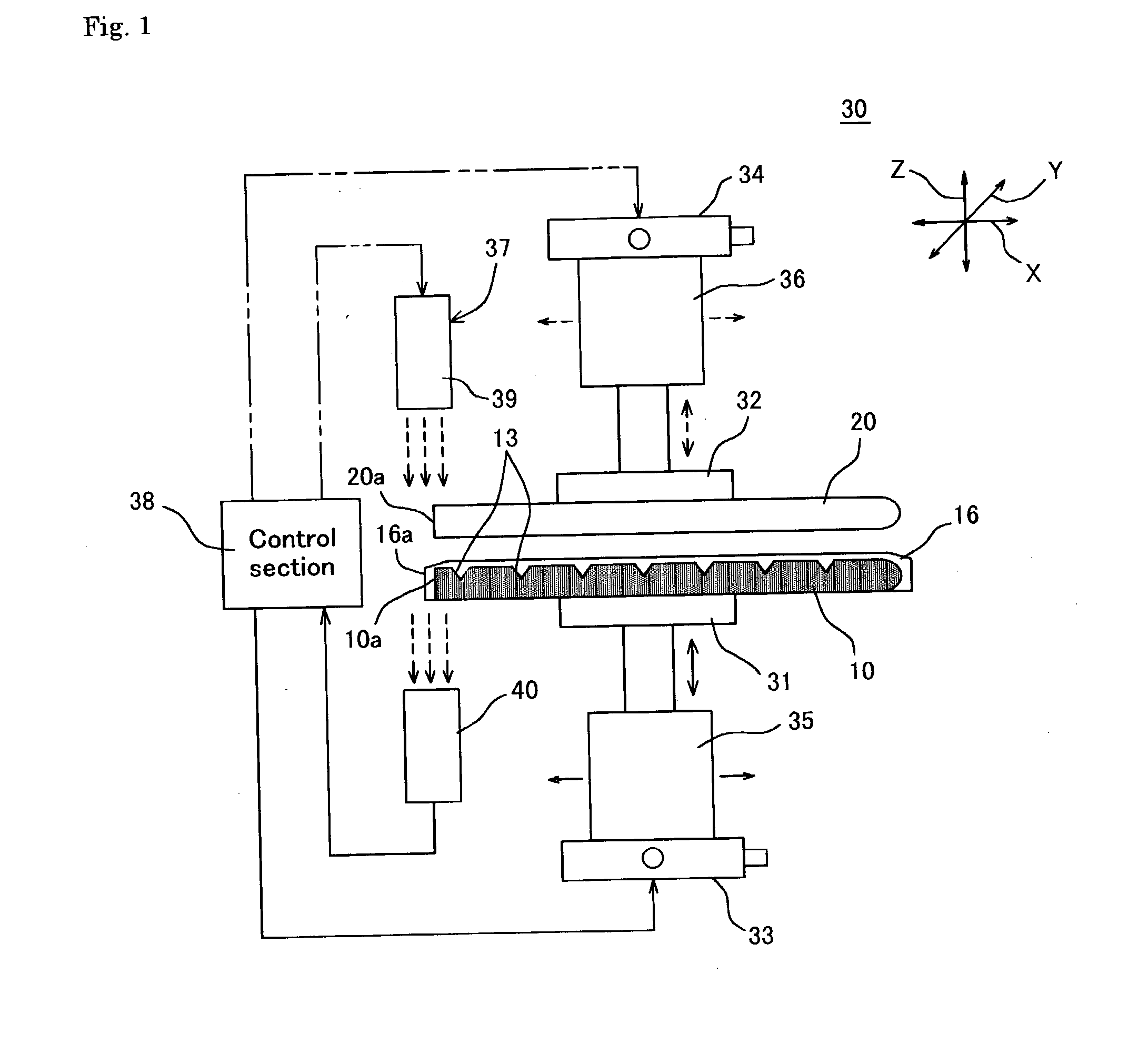
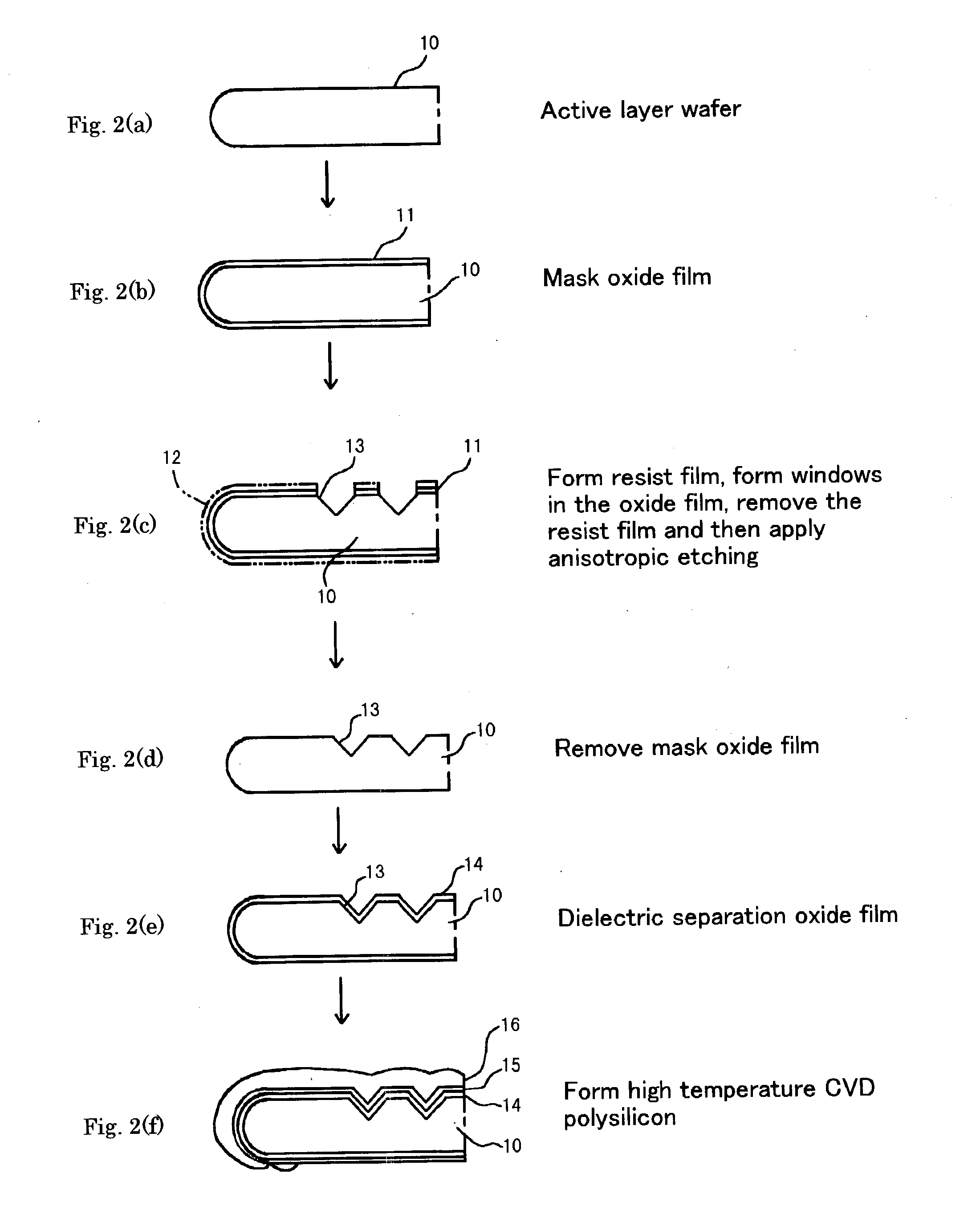
[0049] A method for producing a bonded dielectric separation wafer according to a preferred embodiment of the present invention will now be described. It is to be noted that the explanation in this specification is directed to the method, as an example, for producing a bonded dielectric separation wafer which has been described in connection with the prior art. Accordingly, the same reference numerals are used to designate the same components. For the convenience of the explanation, one direction within a horizontal plane is designated as an X-direction, another direction orthogonal to the X-direction within the horizontal plane as a Y-direction and another direction along a vertical plane as a Z-direction.

[0050] At first, a silicon wafer 10 with a diameter in a range of 4 to 6 inches having a mirror polished surface is fabricated and prepared, which will be formed into an active layer wafer (FIG. 2(a)). A surface orientation should be (100). An orientation flat "OF" (a main flat) h...


PUM


Abstract

The present invention provides a method for producing a bonded dielectric separation wafer in which an auto-alignment can be carried out with reference to the orientation flat of a supporting substrate wafer after the wafer bonding step, and also an apparatus to be used for bonding wafers. When wafers are placed one upon another, the silicon wafers 10, 20 are irradiated with transmission light in order to capture the transmission images thereof. The positions of the pattern of dielectric isolation grooves 13 in the silicon wafer 10 and the orientation flat 20a of the silicon wafer 20 are determined from the images and the bonding position of the wafers 10, 20 is determined based on the determined positions. Auto-alignment of the bonded dielectric separation wafer can thereby be carried out with reference to the orientation flat 20a of the silicon wafer 20 after the wafer bonding step.

Description

[0001] The present invention relates to a method and an apparatus for producing a bonded dielectric separation wafer, and in more specific, to a method for producing such a bonded dielectric separation wafer having a certain physical relationship established between a position of an orientation flat, "OF", of a supporting substrate wafer and a position of a pattern of dielectric isolation grooves of an active layer wafer and also to an apparatus used for bonding those wafers.DESCRIPTION OF THE PRIOR ART[0002] In the prior art, a bonded dielectric separation wafer has been produced through respective steps shown in FIGS. 5 and 6.[0003] In one prior art method, at first, a silicon wafer 10 having a mirror-polished surface is fabricated and prepared in accordance with a well-known method, which will be formed into an active layer wafer (see FIG. 5(a)). This silicon wafer 10 has an orientation flat "OF" formed therein. Secondary, a mask oxide film 11 is formed on a surface of this silic...

Claims


Application Information

Patent Timeline
15 May 2003
Publication
US20030092244A1
IPC
H01L21/02; H01L21/68; H01L21/76; H01L21/762; H01L27/12
CPC
H01L21/681; Y10S438/977; H01L21/76264; H01L21/76256
Inventors
OI, HIROYUKI; OKUDA, HITOSHI