Methods for producing uniform large-grained and grain boundary location manipulated polycrystalline thin film semiconductors using sequential lateral solidification

a polycrystalline thin film, grain boundary location technology, applied in the direction of photomechanical equipment, instruments, manufacturing tools, etc., can solve the problems of poor and non-uniform devices, low manufacturing yield, and difficulty in generating polycrystalline silicon by conventional excimer laser annealing technology

Inactive Publication Date: 2003-05-22
THE TRUSTEES OF COLUMBIA UNIV IN THE CITY OF NEW YORK
View PDF96 Cites 114 Cited by
  • Summary
  • Abstract
  • Description
  • Claims
  • Application Information

AI Technical Summary

Benefits of technology

[0013] In an alternative preferred arrangement, the masking step comprises masking portions of each homoginized fluence controlled laser pulse in the sequence with a two dimensional pattern of substantially parallel straight slits spaced a predetermined distance apart and linearly extending at substantially 45 degree angle with respect to one direction of the plane of homoginization to generate a sequence of fluence controlled pulses of slit patterned beamlets. In this arrangement, the translating step provides for controllably sequentially translating the relative position of the sample in a direction parallel to the one direction of the plane of homoginization over substantially the predetermined slit distance, to thereby process the amorphous silicon thin film sample into polycrystalline silicon thin film having long grained, directionally controlled crystals that are disoriented with respect to the XY axis of the thin silicon film.
[0016] In a modified arrangement, an alternative technique for processing an amorphous silicon thin film sample into a polycrystalline silicon thin film using a polka-dot pattern is provided. Te technique includes generating a sequence of excimer laser pulses, homoginizing each laser pulse in the sequence in a predetermined plane, masking portions of each homoginized laser pulse in the sequence with a two dimensional pattern of substantially opaque dots to generate a sequence of pulses of dot patterned beamlets, irradiating an amorphous silicon thin film sample with the sequence of dot patterned beamlets to effect melting of portions thereof corresponding to each dot patterned beamlet pulse in the sequence of pulses of patterned beamlets, and controllably sequentially translating the sample relative to each of the pulses of dot patterned beamlets by alternating a translation direction in two perpendicular axis and in a distance less than the super lateral grown distance for the sample, to thereby process the amorphous silicon thin film sample into a polycrystalline silicon thin film.

Problems solved by technology

The use of conventional excimer laser annealing technology to generate polycrystalline silicon is problematic for several reasons.
First, the polycrystalline silicon generated in the process is typically small grained, of a random microstructure, and having a nonuniform grain sizes, therefore resulting in poor and nonuniform devices and accordingly, low manufacturing yield.

Method used


Image

  • Methods for producing uniform large-grained and grain boundary location manipulated polycrystalline thin film semiconductors using sequential lateral solidification
  • Methods for producing uniform large-grained and grain boundary location manipulated polycrystalline thin film semiconductors using sequential lateral solidification
  • Methods for producing uniform large-grained and grain boundary location manipulated polycrystalline thin film semiconductors using sequential lateral solidification

Examples


first embodiment

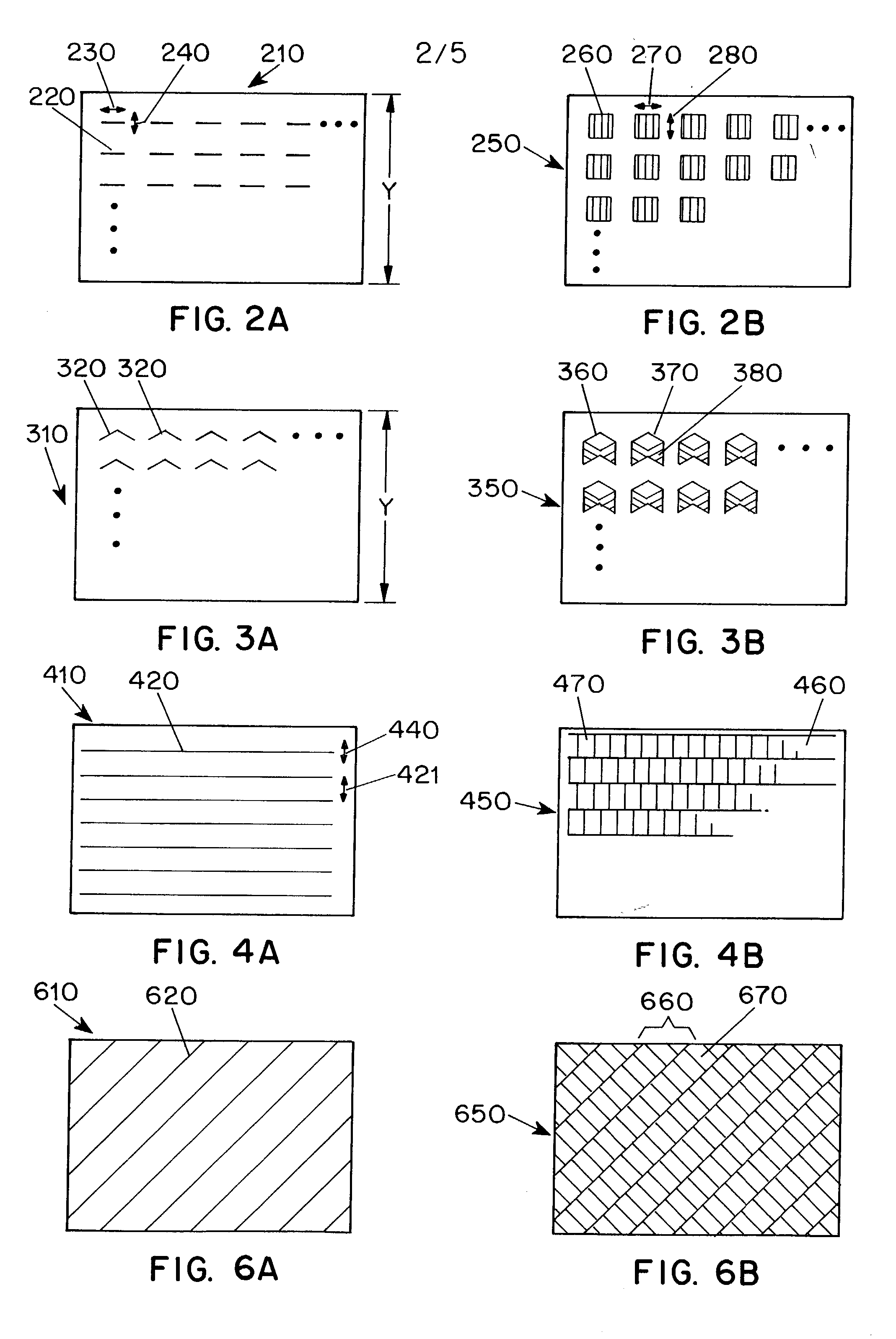
[0044] Referring to FIGS. 2a and b, the present invention will now be described. FIG. 2a illustrates a mask 210 incorporating a pattern of slits 220. The mask 210 is preferably fabricated from a quartz substrate, and includes either a metallic or dielectric coating which is etched by conventional techniques to form a mask pattern, such as that shown in FIG. 2a. Each slit 220 is of a breadth 230 which is chosen in accordance with the necessary dimensionality of the device that will be fabricated on the sample 170 in the particular location that corresponds to the slit 220. For example, the slits 220 should be approximately 25 micrometers across to fabricate a 25 micrometer semiconductor device, or in the case of a multi-part device, a channel in a device, in sample 170. The width 240 of the slit 220 is preferably between approximately two and five micrometers in order to be small enough to avoid nucleation in sample 170 and large enough to maximize lateral crystal growth for each exc...

second embodiment

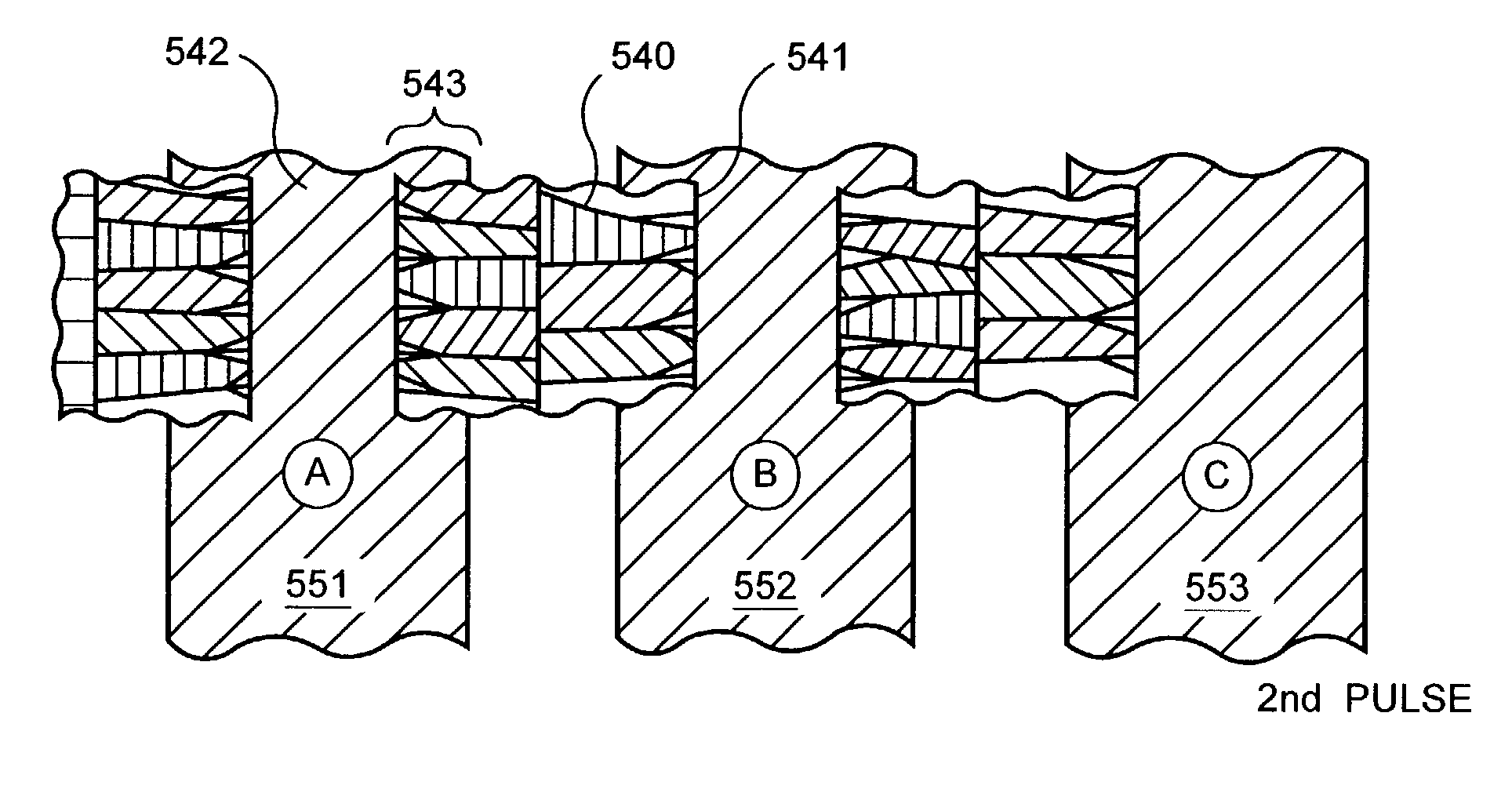
[0046] Referring next to FIGS. 3a and b, the present invention will now be described. FIG. 3a illustrates a mask 310 incorporating a pattern of chevrons 320. The breadth 320 of each chevron side will determine the size of the ultimate single crystal region to be formed in sample 170. When the sample 170 is translated in the Y direction and mask 310 is used in masking system 150, a processed sample 350 having crystallized regions 360 is produced, as shown in FIG. 3b. Each crystal region 360 will consist of a diamond shaped single crystal region 370 and two long grained, directionally controlled polycrystalline silicon regions 380 in the tails of each chevron.

[0047] While the embodiments described with reference to FIGS. 2 and 3 are advantageous to generate spatially separated devices on silicon sample 170, at least some of the silicon sample 170 is not utilized in the final semiconductor. In order to facilitate a more flexible configuration of devices that can be developed on the sem...

third embodiment

[0048] Referring to FIGS. 4a and b, the present invention will now be described. FIG. 4a illustrates a mask 410 incorporating a pattern of slits 410. Each slit 410 should extend as far across on the mask as the homogenized laser beam 149 incident on the mask permits, and must have a width 440 that is sufficiently narrow to prevent any nucleation from taking place in the irradiated region of sample 170. The width 440 will depend on a number of factors, including the energy density of the incident laser pulse, the duration of the incident laser pulse, the thickness of the silicon thin film sample, and the temperature and conductivity of the silicon substrate. For example, the slit should not be more than 2 micrometers wide when a 500 Angstrom film is to be irradiated at room temperature with a laser pulse of 30 ns and having an energy density that slightly exceeds the complete melt threshold of the sample.

[0049] When the sample 170 is translated in the Y direction and mask 410 is used...


PUM

PropertyMeasurementUnit
widthaaaaaaaaaa
widthaaaaaaaaaa
widthaaaaaaaaaa

Abstract

Methods for processing an amorphous silicon thin film sample into a polycrystalline silicon thin film are disclosed. In one preferred arrangement, a method includes the steps of generating a sequence of excimer laser pulses, controllably modulating each excimer laser pulse in the sequence to a predetermined fluence, homoginizing each modulated laser pulse in the sequence in a predetermined plane, masking portions of each homoginized fluence controlled laser pulse in the sequence with a two dimensional pattern of slits to generate a sequence of fluence controlled pulses of line patterned beamlets, each slit in the pattern of slits being sufficiently narrow to prevent inducement of significant nucleation in region of a silicon thin film sample irradiated by a beamlet corresponding to the slit, irradiating an amorphous silicon thin film sample with the sequence of fluence controlled slit patterned beamilets to effect melting of portions thereof corresponding to each fluence controlled patterned beamlet pulse in the sequence of pulses of patterned beamlets, and controllably sequentially translating a relative position of the sample with respect to each of the fluence controlled pulse of slit patterned beamlets to thereby process the amorphous silicon thin film sample into a single or polycrystalline silicon thin film

Description

[0002] I. Field of the Invention[0003] The present invention relates to techniques for semiconductor processing, and more particularly to semiconductor processing which may be performed at low temperatures.[0004] II. Description of the Related Art[0005] In the field of semiconductor processing, there have been several attempts to use lasers to convert thin amorphous silicon films into polycrystalline films. For example, in James Im et al., "Crystalline Si Films for Integrated Active-Matrix Liquid-Crystal Displays," 11 MRS Bullitin 39 (1996), an overview of conventional excimer laser annealing technology is presented. In such a system, an excimer laser beam is shaped into a long beam which is typically up to 30 cm long and 500 micrometers or greater in width. The shaped beam is scanned over a sample of amorphous silicon to facilitate melting thereof and the formation of polycrystalline silicon upon resolidification of the sample.[0006] The use of conventional excimer laser annealing ...

Claims


Application Information

Patent Timeline
Patent Type & Authority Applications(United States)
IPC IPC(8): G03F7/20H01L21/20H01L21/77H01L21/84H01L29/04
CPCB23K26/0626B23K26/063B23K26/0656G03F7/70041G03F7/70725H01L29/04H01L21/0268H01L21/02686H01L21/02691H01L27/1285H01L27/1296H01L21/02532B23K26/0622B23K26/066H01L29/786
Inventor IM, JAMES S.SPOSILI, ROBERT S.CROWDER, MARK A.
Owner THE TRUSTEES OF COLUMBIA UNIV IN THE CITY OF NEW YORK
Why Eureka
Try Eureka