Light emitting devices with improved light extraction efficiency

a technology of light extraction efficiency and light emitting devices, which is applied in the direction of semiconductor devices, electrical equipment, basic electric elements, etc., can solve the problems of compromising the reliability and performance of leds, adding losses due to total internal reflection at the epoxy/air interface, and wasting materials

Inactive Publication Date: 2005-02-03
LUMILEDS
View PDF7 Cites 200 Cited by
  • Summary
  • Abstract
  • Description
  • Claims
  • Application Information

AI Technical Summary

Problems solved by technology

Additional losses due to total internal reflection can occur at the epoxy / air interface.
However, this technique is tedious and wasteful of material.
In addition, defects introduced during the grinding process may compromise the reliability and performance of the LEDs.
However, shaping the surface of a low refractive index encapsulant such as epoxy does not reduce losses due to total internal reflection at the semiconductor / low index encapsulant interface.
Moreover, epoxy encapsulants typically have coefficients of thermal expansion that poorly match those of the semiconductor materials in the LED.
Consequently, the epoxy encapsulant subjects the LED to mechanical stress upon heating or cooling and may damage the LED.
Unfortunately, optical absorption in high index glasses and mechanical stress typically degrade the performance of an LED encapsulated in such glass.

Method used


Image

  • Light emitting devices with improved light extraction efficiency
  • Light emitting devices with improved light extraction efficiency
  • Light emitting devices with improved light extraction efficiency

Examples


Embodiment Construction

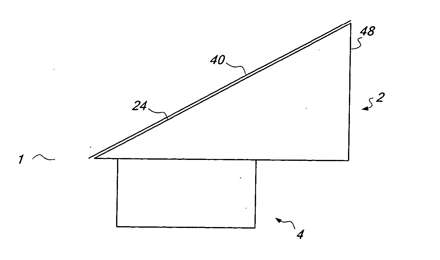
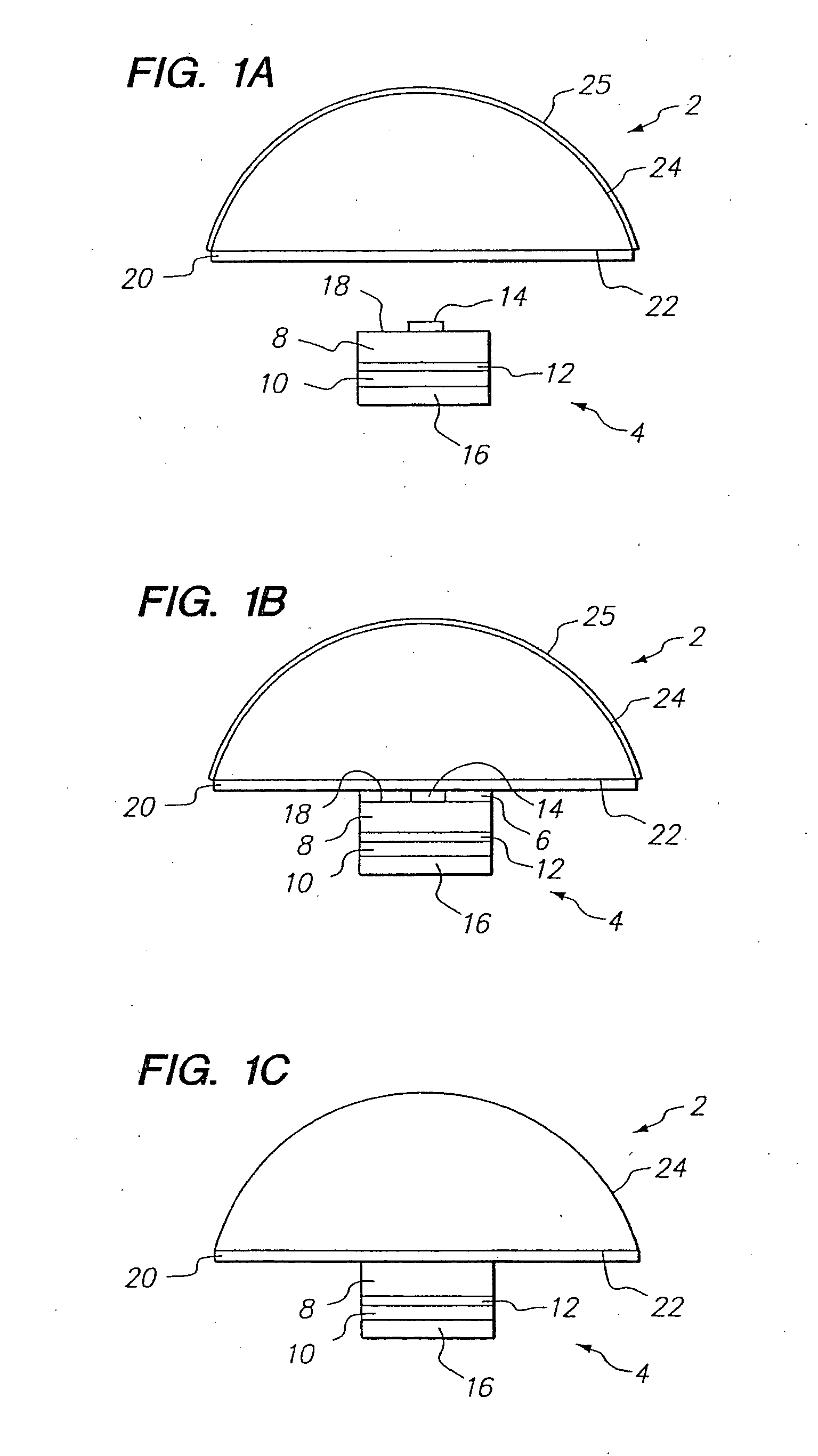
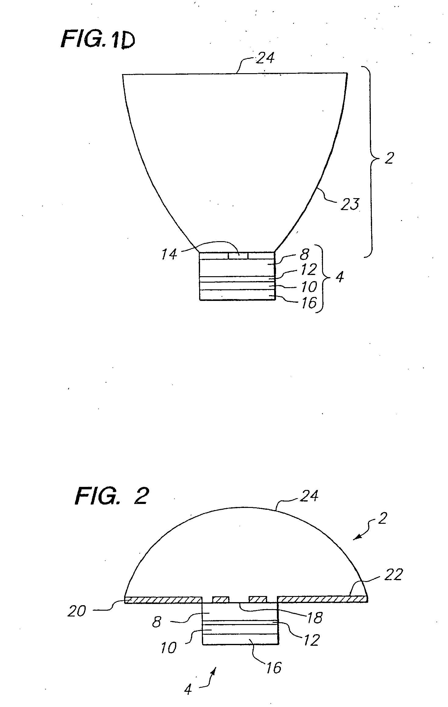
[0030]FIGS. 1-18 illustrate a light emitting device 1, including a substantially transparent optical element 2 bonded to a light emitter 4 according to various embodiments of the invention. The figures describe various light emitters, various optical elements, and various ways to bond the light emitter to the optical element. The particular combinations of light emitter, optical element, and bond illustrated are not meant to be limiting. In general, any of the light emitters, optical elements, and bonds described may be combined. Bonding an optical element to a light emitter may increase the amount of light extracted from the top of the device and the ratio of top light to side light, allowing any optics used with the device to be tailored to top light, possibly resulting in a more efficient and compact system.

[0031]FIG. 1A illustrates optical element 2 and light emitter 4 to be attached by a bond at an interface between light emitter 4 and optical element 2 in accordance with an e...


PUM


Abstract

A device includes a light emitting semiconductor device bonded to an optical element. In some embodiments, the optical element may be elongated or shaped to direct a portion of light emitted by the active region in a direction substantially perpendicular to a central axis of the semiconductor light emitting device and the optical element. In some embodiments, the semiconductor light emitting device and optical element are positioned in a reflector or adjacent to a light guide. The optical element may be bonded to the first semiconductor light emitting device by a bond at an interface disposed between the optical element and the semiconductor light emitting device. In some embodiments, the bond is substantially free of organic-based adhesives.

Description

BACKGROUND OF THE INVENTION DESCRIPTION OF THE RELATED ART [0001] The light extraction efficiency of a light emitter is defined as the ratio of the LED's external quantum efficiency to the LED's internal quantum efficiency. Typically, the light extraction efficiency of a packaged LED is substantially less than one, i.e. much of the light generated in the LED's active region never reaches the external environment. [0002] Light extraction efficiency is reduced by total internal reflection at interfaces between the LED and surrounding material followed by reabsorption of the totally internally reflected light in the LED. For example, for a cubic geometry LED on a transparent substrate encapsulated in epoxy, the refractive index (n) at the emission wavelength changes from a value of, for example, nsemi˜3.5 in the LED semiconductor to nepoxy˜1.5 in the epoxy. The corresponding critical angle for total internal reflection of light incident on the epoxy encapsulant from the LED semiconduct...

Claims


Application Information

Patent Timeline
Patent Type & Authority Applications(United States)
IPC IPC(8): H01L33/44H01L33/58H01L33/60
CPCH01L33/44H01L33/58H01L33/60H01L2924/0002H01L2924/00H01L33/505
Inventor CAMRAS, MICHAEL D.HARBERS, GERARDIMLER, WILLIAM R.KEUPER, MATTHIJS H.MARTIN, PAUL S.POCIUS, DOUGLAS W.STERANKA, FRANK M.TICHA, HELENATICHY, LADISLAVWEST, R. SCOTT
Owner LUMILEDS
Why Eureka
Try Eureka