Printed wiring board and method of manufacturing the same

a technology of printed wiring and wiring board, which is applied in the direction of printed circuit non-printed electric components association, resistive material coating, etching metal masks, etc., can solve the problems of expensive control device for such adjustment, uneven depth accuracy, and complicated laser beam intensity adjustmen

Inactive Publication Date: 2003-08-14
IBIDEN CO LTD
View PDF14 Cites 29 Cited by
  • Summary
  • Abstract
  • Description
  • Claims
  • Application Information

AI Technical Summary

Problems solved by technology

However, these drilling methods cause unevenness in the depth accuracy.
Therefore, it is complicated to adjust the intensity of the laser beam for every via-hole and also requires an expensive control device for such an adjustment.
Since the black oxide film is high in the energy absorption of laser beam, there is a fear of causing damages such as breakage and the like due to fusion and swelling of the innerlayer conductor circuit provided on its surface with the black oxide film.
Also, the insulating layer made of the resin or the like is exposed in the via-hole, so that it is difficult to form the metal plated film.
For this end, the joining property between the inner wall of the via-hole and the metal plated film is low resulting in peeling, dropping-out and the like of the metal plated film.
This can have a bad effect on the electric conduction of the via-hole.
However, as the inner diameter of the hole becomes small, it is difficult to make the formation of the plated film uniform, resulting in the electric conduction of the via-hole being insufficient.
When the diameter of the opening hole is less than 30%, if a distance between the innerlayer conductor circuit having the opening hole and the deepest innerlayer conductor circuit having no opening hole is large, the innerlayer conductor circuit having the opening hole may be damaged by the laser beam.
On the other hand, when it exceeds 60%, the connection between copper plated film and the innerlayer conductor circuit may be insufficient.
Moreover, when the diameter of the flowing hole is less than 0.01 mm, it is feared that the object of flowing the plating solution can not be attained.
While, when it exceeds 0.1 mm, the hole is not closed with the plated film and it is feared to cause a problem that a leakage of a solder is created in the filling of the solder.
On the other hand, when the diameter of the flowing hole is less than 10% of the diameter of the blind via-hole, the flowing of the plating solution may not be attained.
While, when it is more than 40%, the closing of the hole by plating may be insufficient.
On the other hand, when the electroplating treatment is conducted only one time, a long time is taken in the formation of the thick metal plated film.
Therefore, the end portions of the fibers can easily protrude from the wall face of the solder filling hole.
Furthermore, the positioning of the insulating substrates for connecting the through-holes to each other is useless.
However, when it is less than 0.01 mm, the strength at the bottom of the mounting recess portion becomes low and there may be breakage in the heat-sink plate.
However, when it exceeds 2 mm, the working of the heat-sink plate may be difficult.

Method used


Image

  • Printed wiring board and method of manufacturing the same
  • Printed wiring board and method of manufacturing the same
  • Printed wiring board and method of manufacturing the same

Examples


embodiment 11

[0485] Embodiment 11

[0486] A printed wiring board according to the eleventh aspect of the invention is described with reference to FIGS. 40.about.43.

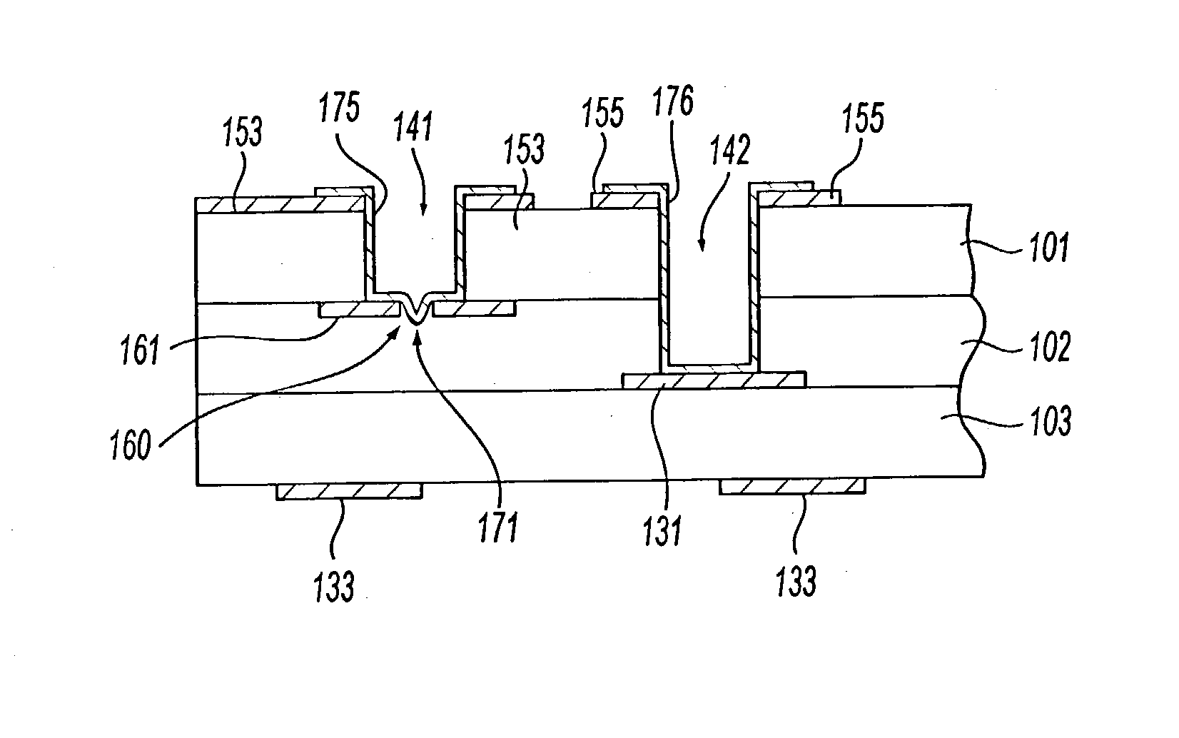
[0487] As shown in FIG. 40, the printed wiring board 802 of this embodiment comprises conductor patterns 851, 852 formed on a surface of a thin insulating substrate 806, and a solder filling hole 801 passing through the insulating substrate 806 and extending to an upper face of the conductor pattern 851. The inside of the solder filling hole 801 is filled with solder paste 807.

[0488] The insulating substrate 806 is formed by impregnating fibers 861 of a glass cloth into epoxy resin 862. As shown in FIGS. 40 and 43, end portions 863 of the fibers 861 protrude from a wall face 810 of the solder filling hole 801. As shown in FIG. 40, the end portions 863 of the fibers 861 encroach into the solder paste 807.

[0489] The insulating substrate 806 is a thin sheet of 0.1 mm in thickness. The solder filling hole 801 has a diameter of 0.3 mm.

[0490]...

embodiment 12

[0502] Embodiment 12

[0503] In a printed wiring board of this embodiment, as shown in FIG. 44, a solder 807 is filled in an inside of a solder filling hole 801 and thereafter a solder ball 871 is adhered to an upper end thereof.

[0504] An upper portion 872 of the solder ball 871 is a portion to be joined to other member 808.

[0505] In the joining of the solder ball 871 to the solder paste 807 inside the solder filling hole 801, as shown in FIG. 45, a lower portion 873 of the solder ball 871 is a flat surface, while an upper portion 872 of the solder ball 871 is spherical.

[0506] Then, the solder ball 871 is placed on the solder paste 807 filled in the inside of the solder filling hole 801 at a state of facing the lower portion 873 of the solder ball 871 thereto likewise Embodiment 11. Next, the solder ball 871 and the solder paste 807 are joined to each other by heat melting.

[0507] Even in this embodiment, the solder paste 807 is strongly adhered to the solder filling hole 801 likewise ...

embodiment 13

[0508] Embodiment 13

[0509] In a printed wiring board of this embodiment, as shown in FIGS. 46 and 47, a ball-shaped solder 870 is fed to an inside of a solder filling hole 801 and melted by heating to fill the solder into the inside of the solder filling hole 801.

[0510] That is, as shown in FIG. 47, the solder filling hole 801 is formed by using the laser beam as in Embodiment 11. The diameter of the solder filling hole 801 is 0.3 mm. Then, a spherical solder ball 870 having a diameter of 0.35 mm is rolled on the surface of the insulating substrate 806 to feed the solder ball 870 to the inside of the solder filling hole 801.

[0511] Next, the solder ball 870 is melted by heating, whereby the end portions 863 of the fibers 861 protruded from the wall face 810 of the solder filling hole 801 encroach into the inside of the solder ball 870 as shown in FIG. 46.

[0512] An upper portion 874 of the solder ball 870 is a portion to be joined to other member 808.

[0513] Even in this embodiment, th...


PUM

PropertyMeasurementUnit
thicknessaaaaaaaaaa
diameteraaaaaaaaaa
diameteraaaaaaaaaa

Abstract

In production of a printed wiring board comprising innerlayer conductor circuits 161, 131 arranged among insulating layers 101~103 and blind via-holes 141, 142 formed from an outermost surface of the insulating layer toward the innerlayer conductor circuit, an opening hole 160 is previously formed in a central portion of the innerlayer conductor circuit 161 located at the bottom of the blind via-hole 141, and laser beams are irradiated from the outermost surface of the insulating layer to form the blind via-holes 141, 142. Thereafter, a metal plated film is formed on surfaces of the innerlayer conductor circuits 131, 161 and the blind via-holes 141, 142.

Description

[0001] 1. Field of Invention[0002] This invention relates to a printed wiring board provided with via-holes formed by using a laser beam and a method of manufacturing the same.[0003] 2. Description of Related Art[0004] A printed wiring board, as shown for example in FIG. 61, is formed by laminating plural insulating layers 91.about.93 one upon the other and electrically connecting innerlayer conductor circuits 95, 97 arranged between the layers to an outer conductor circuit 94 existing on an outermost surface through metal plated films 96 formed on via-holes 99a, 99b. A resin substrate such as glass-epoxy substrate or the like is used to form insulating layers 91-93. The via-holes 99a, 99b are blind via-holes each covered at one end and opened at the other end.[0005] There are various methods of forming via-holes, such as using a drill, using a laser beam, etc.[0006] However, these drilling methods cause unevenness in the depth accuracy. And also, it is recently demanded to make mor...

Claims


Application Information

Patent Timeline
Patent Type & Authority Applications(United States)
IPC IPC(8): B23K26/00H01L21/48H05K1/02H05K1/03H05K1/11H05K1/18H05K3/00H05K3/34H05K3/38H05K3/40H05K3/42H05K3/46
CPCH01L21/486Y10T29/49155H01L2224/48227H01L2924/01039H01L2924/01078H01L2924/01079H01L2924/15153H01L2924/1517H05K1/0203H05K1/021H05K1/0271H05K1/0366H05K1/112H05K1/116H05K1/182H05K3/0035H05K3/0061H05K3/3468H05K3/3484H05K3/385H05K3/4038H05K3/421H05K3/423H05K3/427H05K3/428H05K3/429H05K3/4602H05K3/4611H05K3/4652H05K2201/0305H05K2201/0394H05K2201/09472H05K2201/09509H05K2201/09518H05K2201/0969H05K2201/09781H05K2201/09845H05K2201/09854H05K2201/09863H05K2203/0315H05K2203/041H05K2203/0554H01L2224/48091Y10T29/49165H01L2924/00014H05K3/3485H05K3/46
Inventor TAKADA, MASARUTSUKADA, KIYOTAKAKOBAYASHI, HIROYUKIMINOURA, HISASHIUKAI, YOSHIKAZUKONDO, MITSUHIRO
Owner IBIDEN CO LTD
Why Eureka
Try Eureka