
Use of printing and other technology for micro-component placement
a technology of micro-components and printing, applied in the field of lightemitting panels, can solve the problems of high cost of ito, high cost of final plasma display, and high cost of manufacturing process and ultimately final plasma display
- Summary
- Abstract
- Description
- Claims
- Application Information
AI Technical Summary
Benefits of technology
Problems solved by technology
Method used
Image

Examples
Embodiment Construction
[0062] As embodied and broadly described herein, the preferred embodiments of the present invention are directed to a novel light-emitting panel. In particular, preferred embodiments are directed to light-emitting panels and to a web fabrication process for manufacturing light-emitting panels.
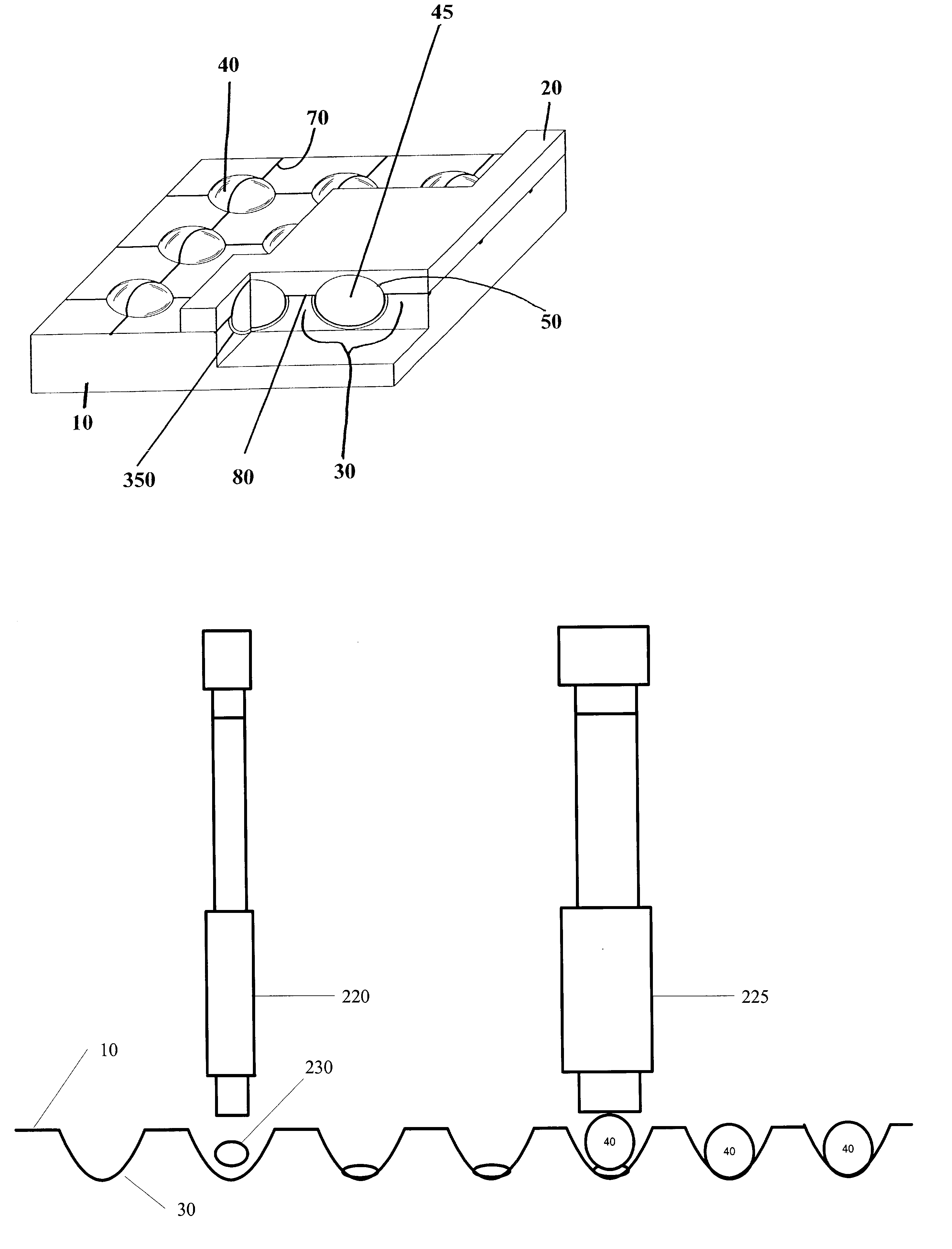
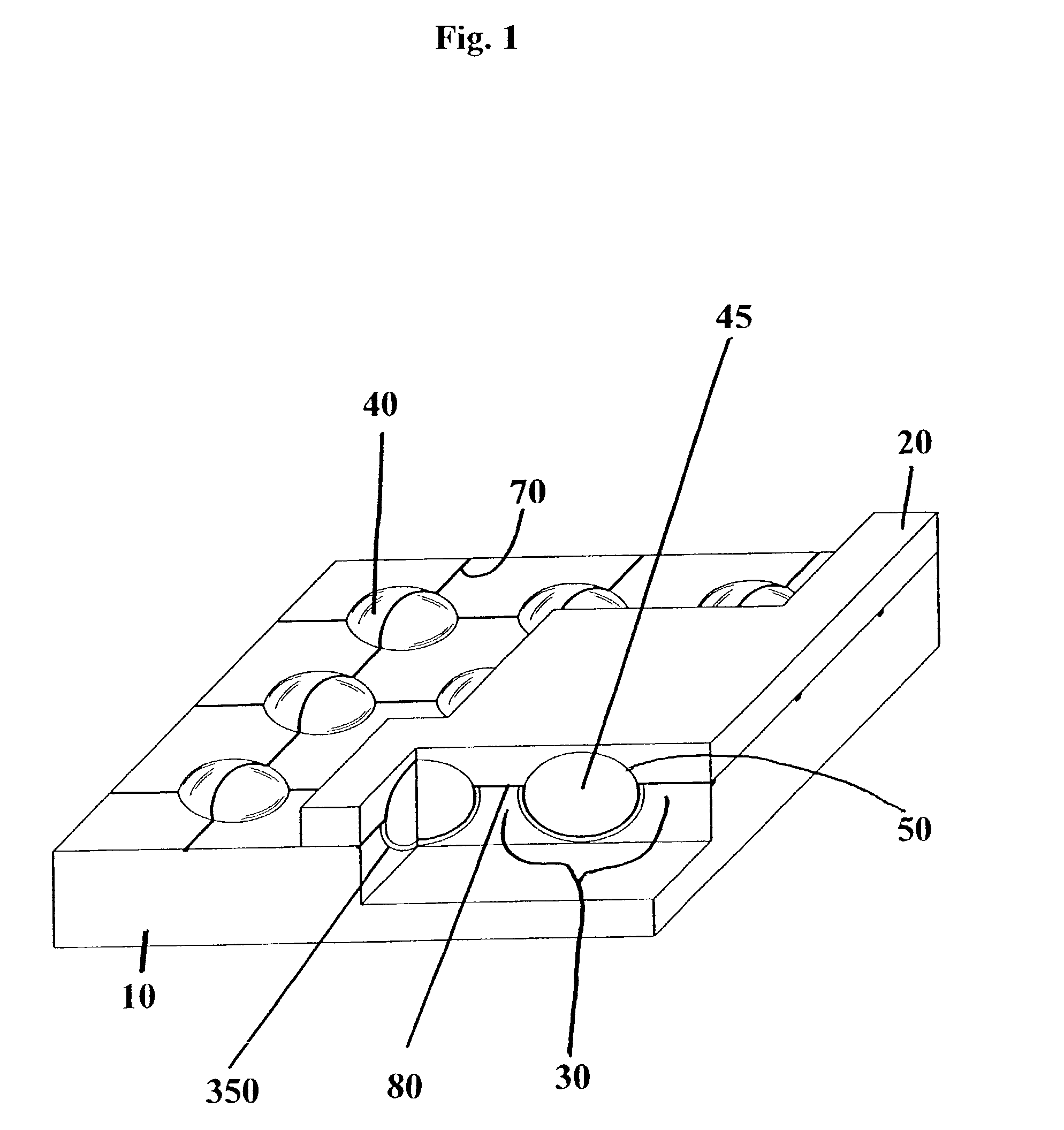
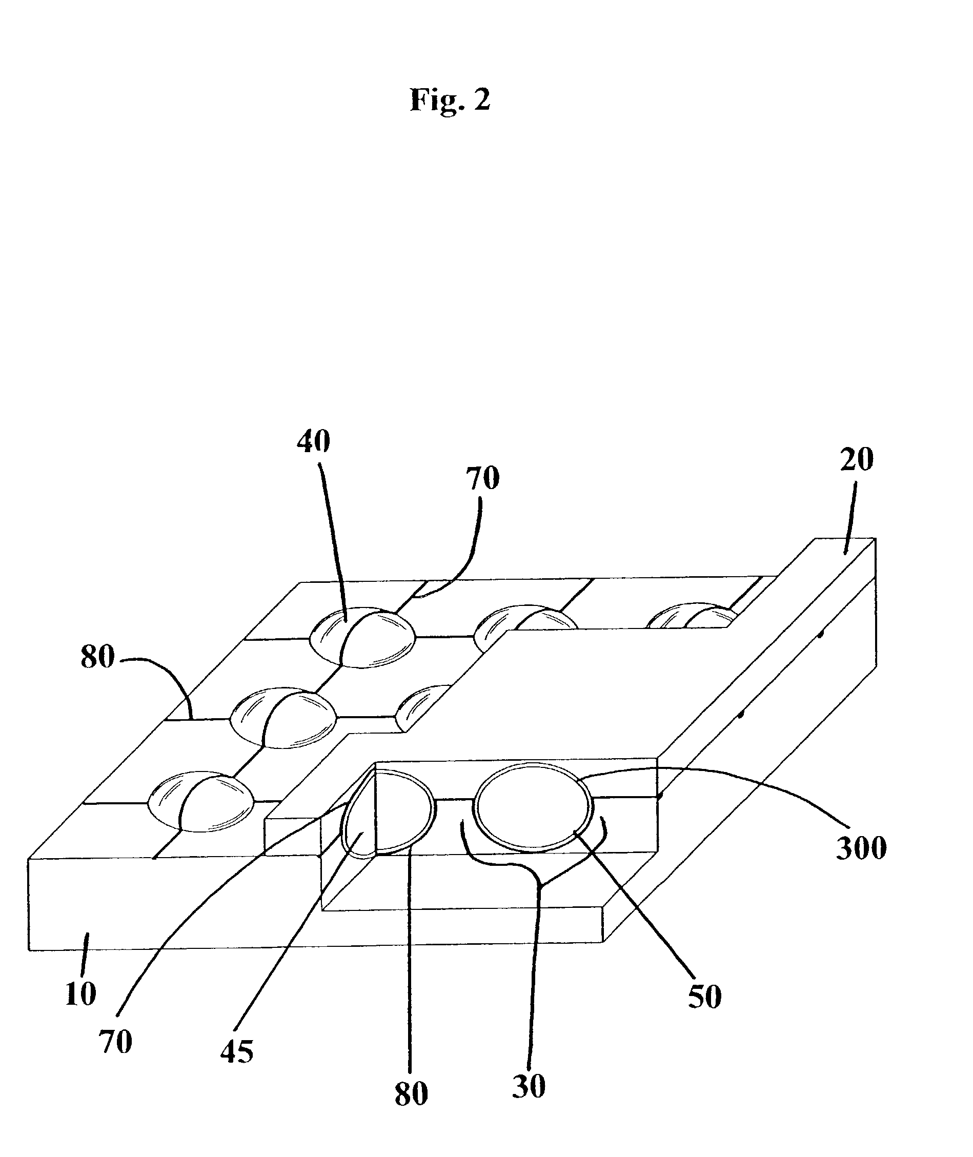
[0063] FIGS. 1 and 2 show two embodiments of the present invention wherein a light-emitting panel includes a first substrate 10 and a second substrate 20. The first substrate 10 may be made from silicates, polypropylene, quartz, glass, any polymeric-based material or any material or combination of materials known to one skilled in the art. Similarly, second substrate 20 may be made from silicates, polypropylene, quartz, glass, any polymeric-based material or any material or combination of materials known to one skilled in the art. First substrate 10 and second substrate 20 may both be made from the same material or each of a different material. Additionally, the first and second substrate may b...
PUM
| Property | Measurement | Unit |
|---|---|---|
| radiating wavelengths | aaaaa | aaaaa |
| radiating wavelengths | aaaaa | aaaaa |
| diameter | aaaaa | aaaaa |
Abstract
Description
Claims
Application Information