Chip mounting device and callibration method therein
- Summary
- Abstract
- Description
- Claims
- Application Information
AI Technical Summary
Benefits of technology
Problems solved by technology
Method used
Image
Examples
Embodiment Construction
[0030] Hereinafter, desirable embodiments of the present invention will be explained referring to figures.
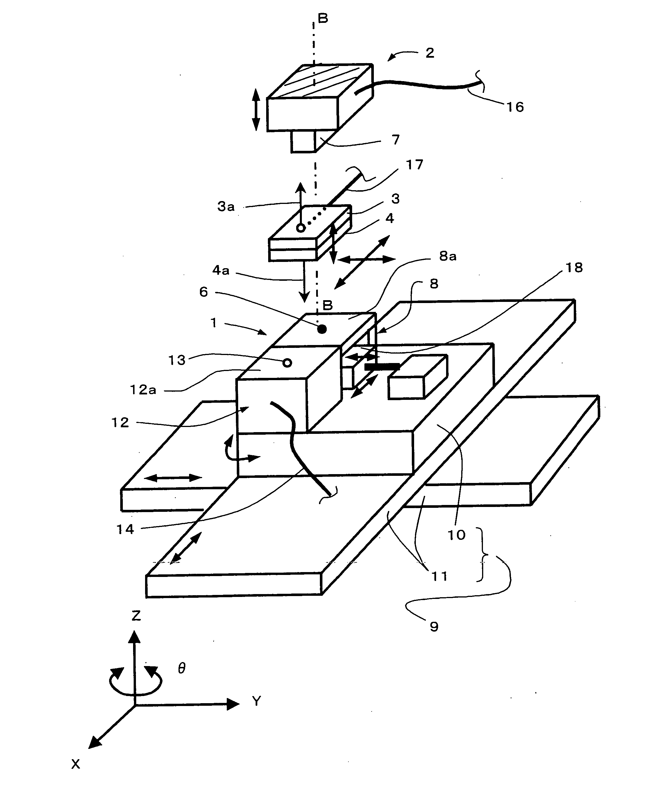
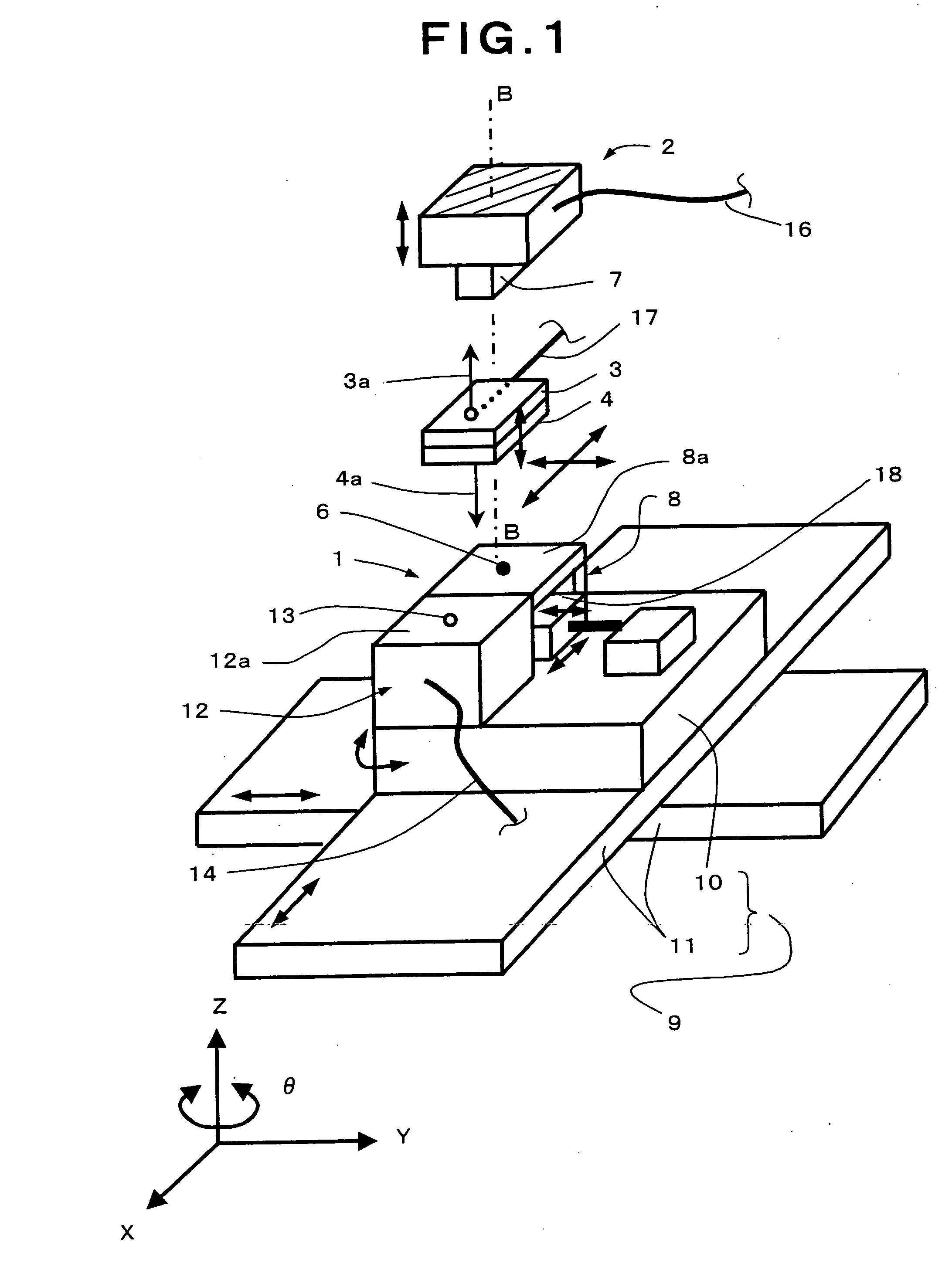
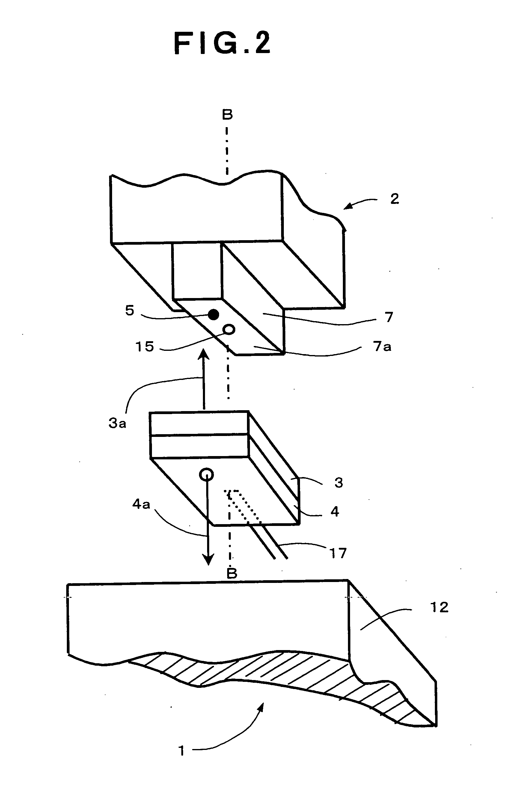
[0031] FIGS. 1 and 2 show a chip mounting device according to an embodiment of the present invention. In FIGS. 1 and 2, a state is shown wherein a first recognition means 3 (for example, a CCD camera) and a second recognition means 4 (for example, a CCD camera) are moved to a position between a lower stage 1 and an upper head 2, and the first recognition means 3 and the second recognition means 4 are attached so as to be integrally moved, namely, attached in a form of a two-sight recognition means.
[0032] Therefore, first recognition means 3 can recognize a first recognition mark 5 of upper side, and second recognition means 4 can recognize a second recognition mark 6 of lower side. First recognition mark 5 is provided on a pressing surface 7a of a tool 7 forming a tip portion of head 2, and second recognition mark 6 is provided on an upper surface 8a of a mark recognition part 8...
PUM
| Property | Measurement | Unit |
|---|---|---|
| Temperature | aaaaa | aaaaa |
Abstract
Description
Claims
Application Information


