Multiprobe blob test in lieu of 100% probe test

a technology of blob test and probe test, which is applied in the direction of semiconductor/solid-state device testing/measurement, instruments, nuclear elements, etc., can solve the problems of adding additional cost, increasing the cost of wafer test, and adding significant cost to the wafer

Inactive Publication Date: 2004-02-19
TEXAS INSTR INC
View PDF3 Cites 3 Cited by
  • Summary
  • Abstract
  • Description
  • Claims
  • Application Information

AI Technical Summary

Benefits of technology

0016] In accordance with an embodiment of the present invention a method of predicting the effect of blob test in GSP sample testing includes the steps of extracting failure density maps from sample test results, where the density of any failed cell is expressed as the number of adjacent failing sample cells; determining the existence of local concentration of bad chips (blobs) as the occurrence of a detection density value above a threshold which can be adjusted to control the sensitivity of blob detection; determining the extent of such identified blobs as the occurrence of adjacent cells with density values above an inclusion threshold, which can also be adjusted to control the sensitivity of blob extent determination; calculating a residual sample yield Y.sub.NB for the areas outside blob regions using the total sample cell count N.sub.S, the passing cell count N.sub.G, and the count of cells in blobs N.sub.B by equation: 2 Y NB = N GN S - N B ;

Problems solved by technology

Wafer testing adds a significant cost to the wafers and when chip yields are very high, the cost of wafer test is more than the resultant cost that would result from assembly of small number of non-functional circuits.
Since this yield threshold is high, a significant number of wafers must be fully tested adding extra cost, decreasing test capacity and hampering production planning by introducing variability in manufacturing cycle time.
All other grey shades are test failures.

Method used


Image

  • Multiprobe blob test in lieu of 100% probe test
  • Multiprobe blob test in lieu of 100% probe test
  • Multiprobe blob test in lieu of 100% probe test

Examples


Embodiment Construction

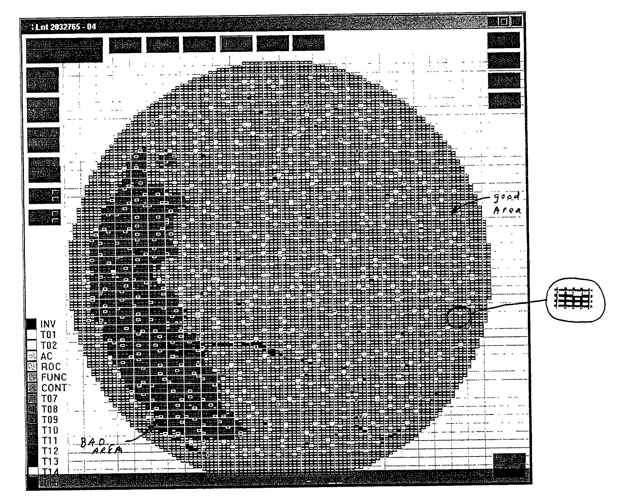
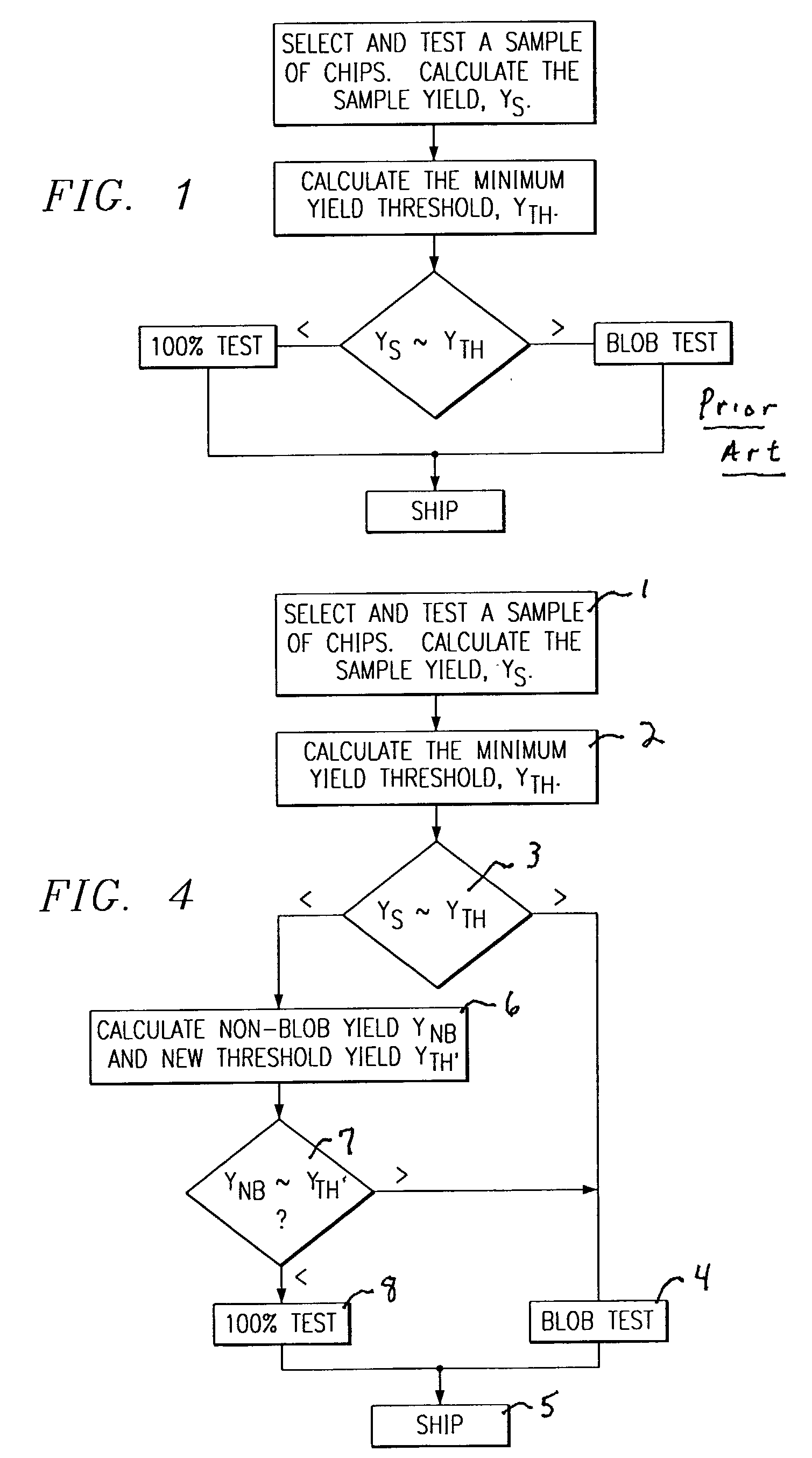
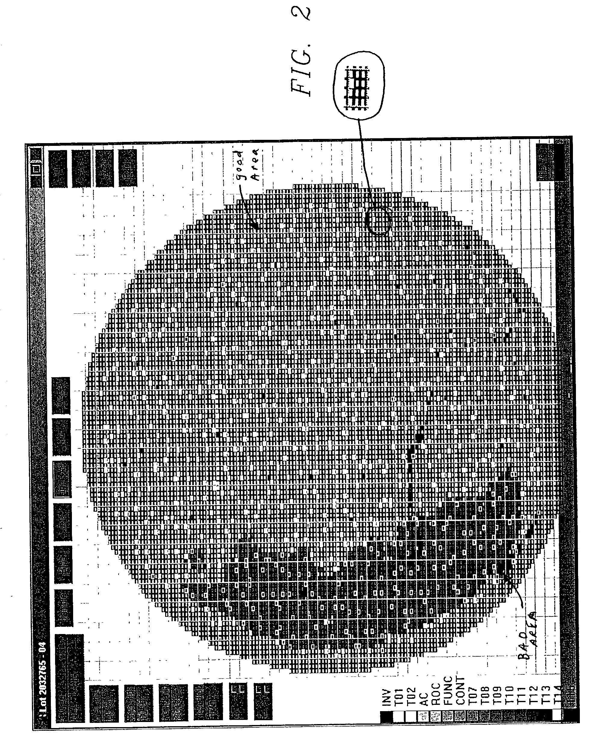
[0027] Many wafers with relatively low yield have one or more localized concentrations, or blobs of bad chips, while the remainder of the wafer has relatively few bad chips. After sample testing, the sample yield indicates that 100% test would be less costly than assembly of untested (not sampled) chips that will subsequently fail final test. The present invention is a method for identifying when blob test, as described above would be sufficient to reduce the number of untested bad chips to a level where a cost savings can still be realized. Some wafers which fail the sample test yield threshold do so because of one or more local concentrations, or blobs, of bad chips. In many cases, most or all chips in a region are bad and blob test would suffice to test out the majority of bad chips without the need for 100% test.

[0028] The method by which this is accomplished is by analyzing the sample results to (1) identify blobs that will be tested out by the blob test, (2) estimate the yield...


PUM

PropertyMeasurementUnit
yield thresholdaaaaaaaaaa
residual yieldaaaaaaaaaa
failure densityaaaaaaaaaa

Abstract

A method of predicting the effect of blob test in GSP sample testing is disclosed. The method includes extracting failure density maps from sample test results, where the density of any failed cell is expressed as the number of adjacent failing sample cells; determining the existence of local concentration of bad chips (blobs) as the occurrence of a detection density value above a threshold which can be adjusted to control the sensitivity of blob detection; determining the extent of such identified blobs as the occurrence of adjacent cells with density values above an inclusion threshold, which can be adjusted to control the sensitivity of blob extent determination; calculating a residual sample yield YNB for the areas outside blob regions using the total sample cell count NS, the passing cell count NG, and the count of cells in blobs NB by equation: <math-cwu id="MATH-US-00001"> <NUMBER>1</NUMBER> Y NB = N G N S - N B ; <mathematica-file id="MATHEMATICA-00001" file="US20040034493A1-20040219-M00001.NB"/> <image id="EMI-M00001" wi="216.027" he="18.96615" file="US20040034493A1-20040219-M00001.TIF" imf="TIFF" ti="MF"/> </MATH-CWU> and re-evaluating the decision of whether 100% probe test is required or if the cost savings can still be realized by performing only blob test.

Description

[0001] This invention relates to testing semiconductor wafers and more particularly to determining the cost savings of a multiprobe sample (blob) test in lieu of 100% probe test.BACKGROUND OF INVENTION[0002] Massive quantities of completed fabricated integrated circuits are functionally tested by being probed in wafer form by multiprobe test device before separation and encapsulation of the integrated circuits into individual packages (assembly). Since the circuits are again tested after assembly and before shipment to customers, the justification for probing wafers is to avoid the cost of assembly on non-functional circuits. Wafer testing adds a significant cost to the wafers and when chip yields are very high, the cost of wafer test is more than the resultant cost that would result from assembly of small number of non-functional circuits. A sample test procedure is therefore employed to identify wafers with high enough yield to allow cost effective avoidance of 100% test. The yiel...

Claims


Application Information

Patent Timeline
Patent Type & Authority Applications(United States)
IPC IPC(8): G01R31/28
CPCG01R31/2831
Inventor STUBBLEFIELD, TODD D.GHARIS, EUGENE T.REEVES, GEORGE W.
Owner TEXAS INSTR INC
Why Eureka
Try Eureka