Method for selectively transferring at least an element from an initial support onto a final support

a technology of at least an element and a transfer support, which is applied in the direction of lasers, semiconductor laser structural details, sensing record carriers, etc., can solve the problems of not being compatible with the standard micro-electronic equipment, not enabling us to handle individual components of small dimension or extreme thinness, and not enabling us to transfer elements strongly adhered to the transfer suppor

Inactive Publication Date: 2004-06-03
COMMISSARIAT A LENERGIE ATOMIQUE ET AUX ENERGIES ALTERNATIVES
View PDF9 Cites 23 Cited by
  • Summary
  • Abstract
  • Description
  • Claims
  • Application Information

AI Technical Summary

Problems solved by technology

This latter method does not enable us to handle individual components of small dimension or extreme thinness as with the two previous ones.
The method described in that document does not enable us to transfer elements strongly adhered on the transfer support, for example, at energy above 200 mJ/m.sup.2.
In addition, it is not compatible with the standard micro-electronic equipment such as the "pick and place" equipment.
This method does not allow the selective transfer of an element in thin layer.
However, due to the lateral under-engraving of the sacrificial layer, the dimensions of the chips to be transferred are limited.
It is obvious that the epitaxial growth of t

Method used


Image

  • Method for selectively transferring at least an element from an initial support onto a final support
  • Method for selectively transferring at least an element from an initial support onto a final support
  • Method for selectively transferring at least an element from an initial support onto a final support

Examples


Embodiment Construction

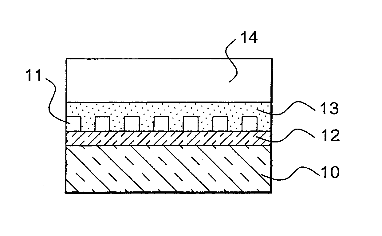
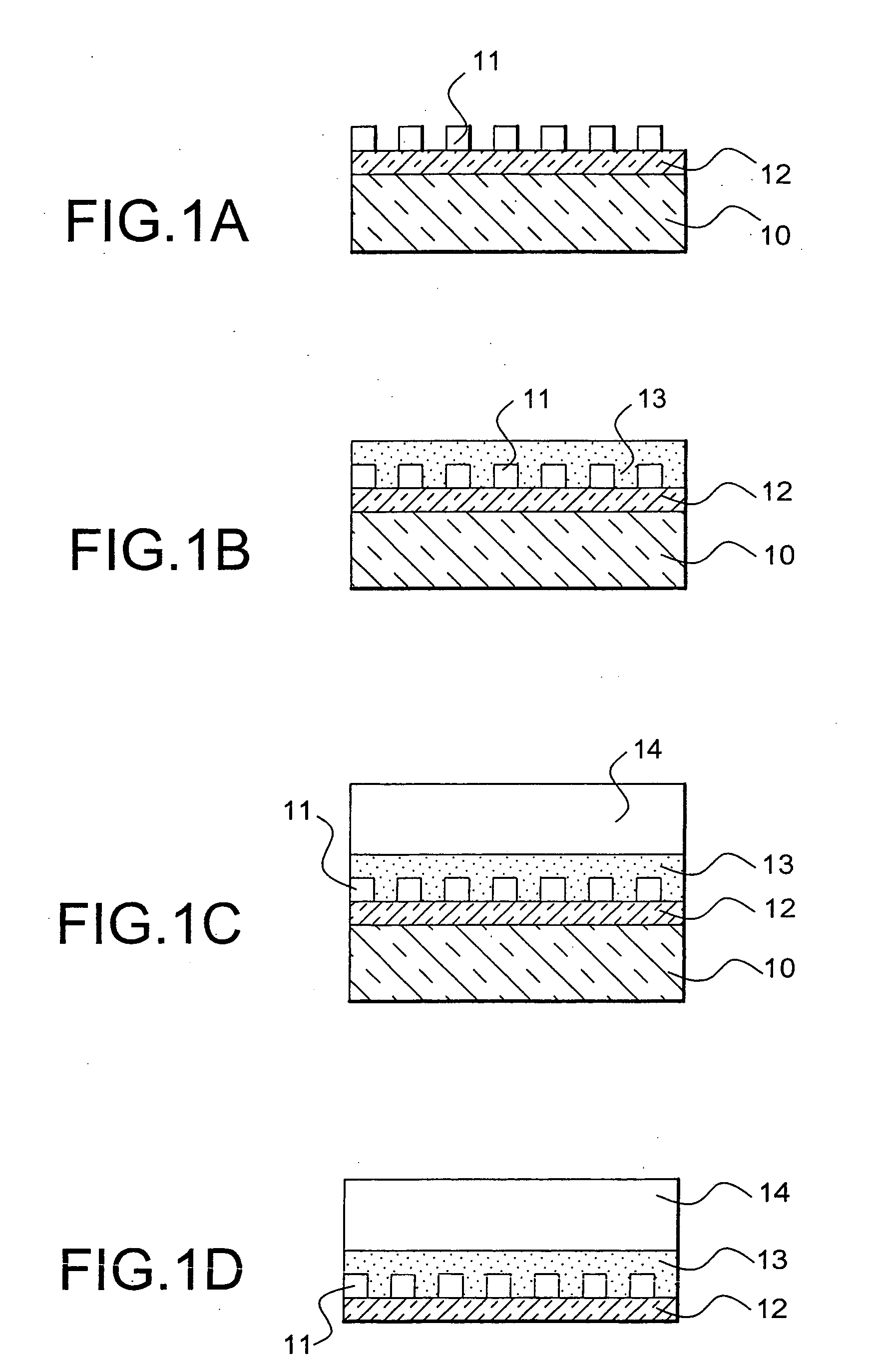
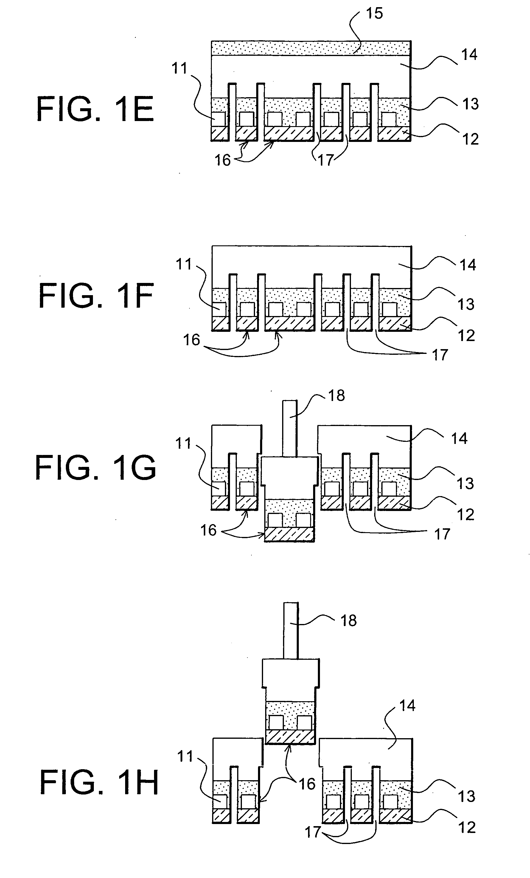
[0055] Generally speaking, the process applies to elements fully or partially made on substrates by the techniques of microelectronics and / or optoelectronics. The elements can possibly be made on one or several layers of chemical stoppage. They can possibly be subjected to an electric test on their initial support.

[0056] In case there exists a strong surface topology, a polishing of the surface can be carried out by the deposit of material followed by a chemical-mechanical polishing or by filling the volumes with a material sufficiently smooth that does not require any subsequent polishing. If the layer of filling material is sufficiently thick and rigid, it can also fulfil a function of rigidification and make up the transfer support. In addition, it can, when necessary, fulfil an adhesion function.

[0057] Different techniques can be used to fix the transfer support on the initial support: molecular adhesion, glue, epoxy resin, etc. The molecular adhesion is particularly appropriate...


PUM


Abstract

The invention concerns a process of selective transfer of labels from an initial support to a final support, each label including at least one element constituent of a microelectronic and/or optoelectronic and/or acoustic and/or mechanical device, with the elements made in a surface layer of the initial support, and the process including the following stages: a) Fixing a transfer support on the surface layer of the initial support; b) Eliminating the part of the initial support that does not correspond to the surface layer; c) Laterally defining the labels by cutting according to the thickness of the surface layer, with the cutting leaving zones to be broken off; d) Grasping one or several labels to be transferred and tearing them off by means of energy intake in the corresponding zones that can be broken off; e) Transfer and fixing the label or set of labels torn off in stage d) on the final support.

Description

DESCRIPTION[0001] 1--Field of the Invention[0002] The abovementioned invention concerns the selective transfer of one or several elements we can call labels, from a manufacturing support to a receiving support.[0003] It concerns, in particular, the transfer of semi-conducting chips, partially or fully completed, from their initial substrate on which they are manufactured to a new substrate (or receiving support) that can itself be treated by microelectronic techniques.[0004] The invention enables us, in particular, to transfer chips that may have been electronically tested, for example, chips of 1 mm.sup.2 to 1 cm.sup.2 area, from their initial substrate to a support made of treated or non-treated semi-conducting material, transparent material, (example: glass), a soft or rigid support (example: plastic) or a support made of ceramics. It also enables us, for example, to transfer optoelectronic components such as a vertical cavity surface emitting lasers or VCSEL or small pieces of I...

Claims


Application Information

Patent Timeline
IPC IPC(8): H01L21/02H01L21/52H01L21/68H01L21/98H01S5/02
CPCH01L21/6835H01L24/97H01L2924/10253H01L25/50H01L2221/68359H01L2221/68368H01L2224/83894H01L2924/01004H01L2924/01013H01L2924/01015H01L2924/01033H01L2924/01057H01L2924/01058H01L2924/01074H01L2924/01075H01L2924/01079H01L2924/01082H01L2924/01094H01L2924/09701H01L2924/10329H01L2924/19043H01L2924/30105H01S5/0201H01S5/0202H01S5/0215H01S5/0217H01L2924/01005H01L2924/01006H01L2924/01019H01L2924/01023H01L2924/01087H01L2924/00H01L2924/12042H01L21/68
Inventor FIGUET, CHRISTOPHEASPAR, BERNARDBLET, VINCENT
Owner COMMISSARIAT A LENERGIE ATOMIQUE ET AUX ENERGIES ALTERNATIVES
Why Eureka
Try Eureka