Light-emitting diode

a technology of light-emitting diodes and diodes, which is applied in the direction of basic electric elements, electrical equipment, semiconductor devices, etc., can solve the problems of insufficient light-emission efficiency, insufficient concentration current area, and difficult to make light-emission wide and uniform in an led

Active Publication Date: 2004-07-01
NICHIA CORP
View PDF4 Cites 52 Cited by
  • Summary
  • Abstract
  • Description
  • Claims
  • Application Information

AI Technical Summary

Problems solved by technology

However, it is not easy to make light-emission wide and uniform in an LED, even though the p-side current diffusing member is provided in the p-side electrode.
That is a first problem.
On the other hand, when each electrode is deformed or enlarged in order to make light-emission wide, this causes too high a concentration current area.
Consequently, this causes not only insufficient efficiency of light-emission efficiency but also reduction of the life.
Furthermore, when an opening portion is provided in an area which is usually a light-emission area in order to improve light-emitting efficiency, this reduces device characteristics such as high LED resistance.
That is a second problem.

Method used


Image

  • Light-emitting diode
  • Light-emitting diode
  • Light-emitting diode

Examples


embodiment 1

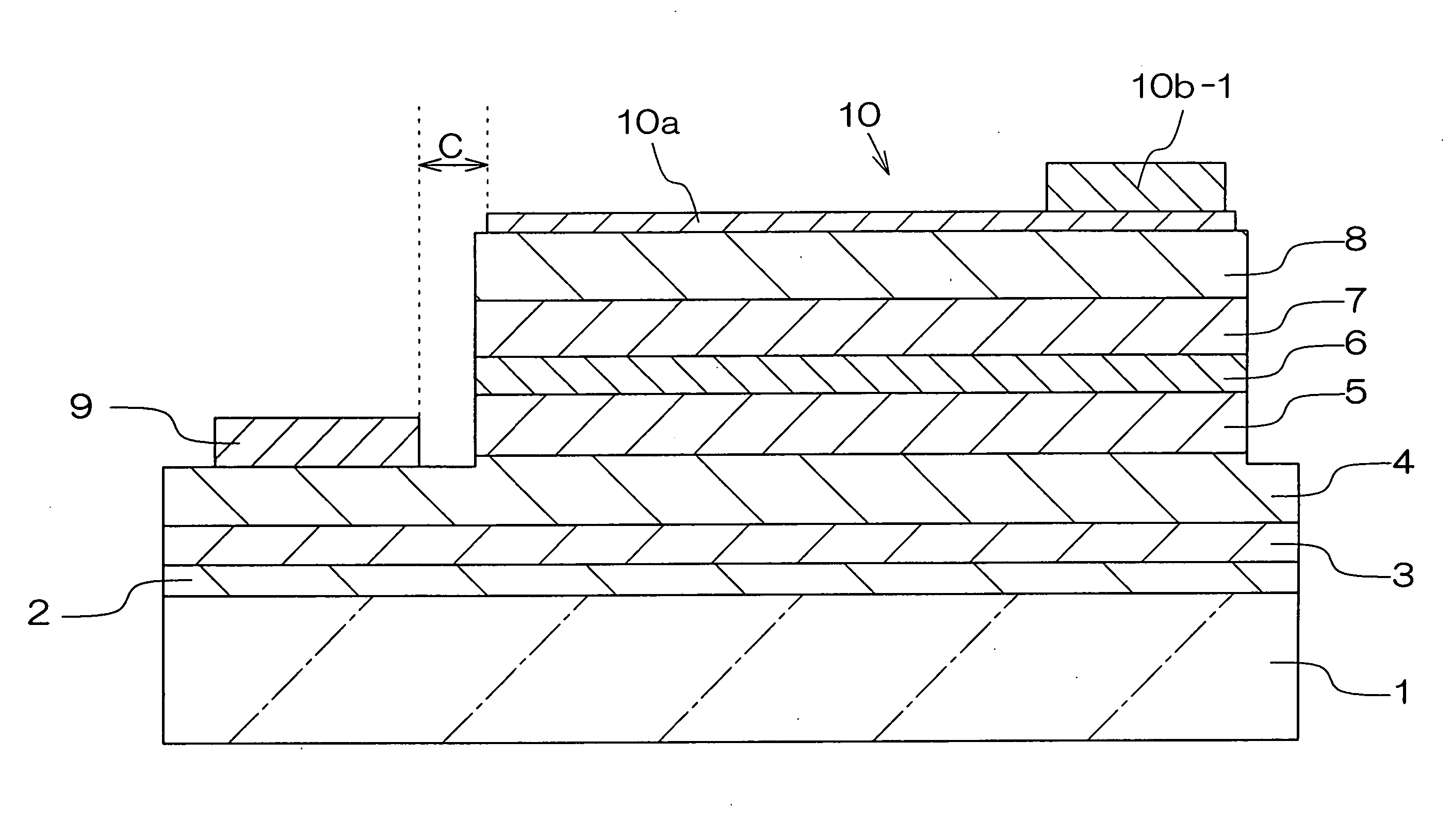
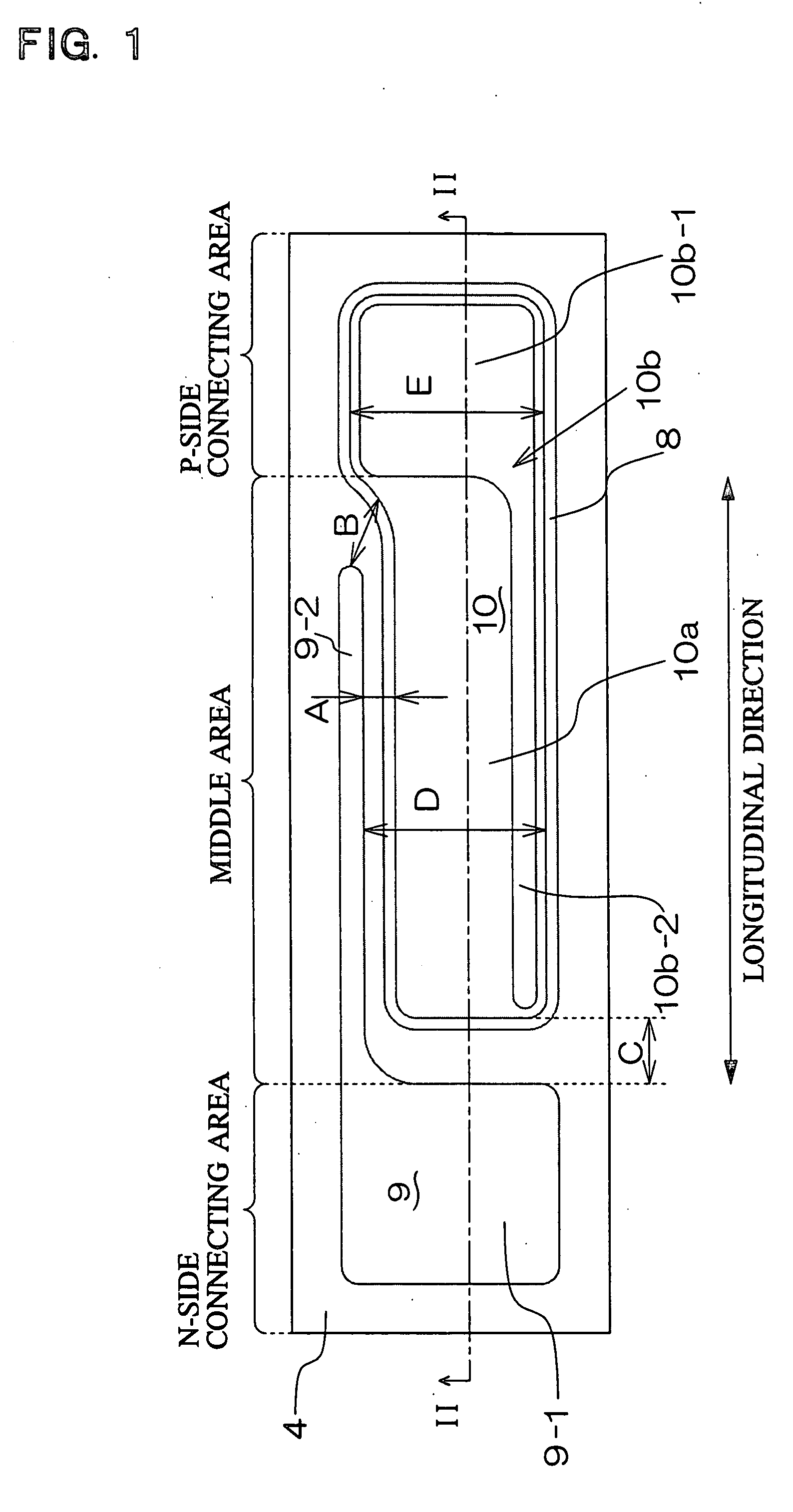
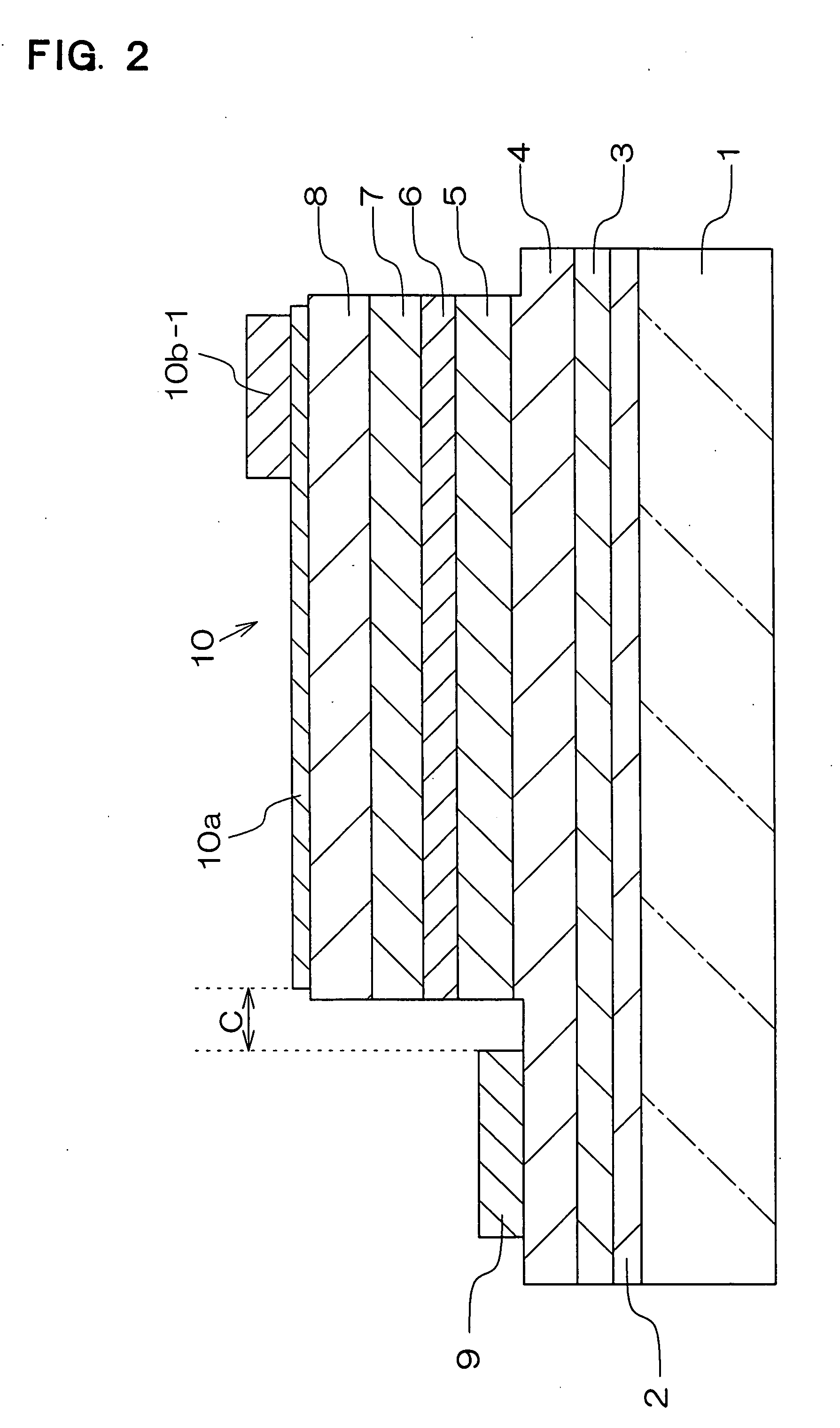
[0044] The following description will describe an LED of the embodiment 1 with reference to FIG. 1 and FIG. 2. As shown in these drawings, the LED of this embodiment has a p-side electrode and an n-side electrode positioned in the same plane side. FIG. 1 is a schematic diagram showing the LED of this embodiment in view from an electrode-forming-plane side. FIG. 2 is a cross-sectional view schematically showing layer construction of the LED of this embodiment of FIG. 1 taken along the line II-II.

[0045] As shown in FIG. 1, the LED of the embodiment 1 according to the present invention has a shape with a longitudinal direction, which is a predetermined direction, in the view from the electrode-forming-plane side. In this embodiment, the shape is a rectangle, in which one pair of sides is longer than another pair of sides. An n-side connecting portion 9-1 is positioned in proximity to one end in the longitudinal direction of the rectangle. A p-side connecting portion 10b-1 is positioned...

embodiment 2

[0072] The following description will describe an LED of the embodiment 2 with reference to FIG. 3 and FIG. 4. FIG. 3 is a schematic diagram showing the LED of this embodiment in view from an electrode-forming-plane side. FIG. 4 is a cross-sectional view schematically showing layer construction of the LED of this embodiment of FIG. 3 taken along the line IV-IV. In addition, the same reference signs show the members of similar function in the embodiment 1.

[0073] The LED of this embodiment has the same construction mentioned as the LED of the embodiment 1 except that the p-side current diffusing member 10a has a plurality of openings 10aa. In addition, the p-side pad member does not have the p-side extending portion. In this case, the p-side extending portion does not cut off the light emitted from the active layer. Such a construction is preferable in view of light outgoing. Needless to say, the LED can also have the p-side extending portion in view of current diffusing. A designer c...

embodiment 3

[0081] The following description will describe an LED of the embodiment 3 with reference to FIG. 5 and FIG. 6. In addition, the same reference signs show the members of similar function in the embodiment 1. The LED of this embodiment has the same construction mentioned as the LED of the embodiment 1 except the members described bellow.

[0082] In the LED of this embodiment, as mentioned above, the p-side current diffusing member 10a is formed also in the n-side connecting area. The n-side pad member 9-1 and the p-side pad member 10b-1 are positioned at opposite corners of the LED with a rectangular shape in view from the electrode-forming-plane side. In addition, the n-side extending portion 9-2 and the p-side extending portion 10b-2 are partially opposed to each other. Additionally, a plurality of bumps 11, which improves light outgoing, are provided in the area, in which the n-type contact portion 4 is exposed in order to form the n-side electrode, so as to surround the laminated-la...


PUM


Abstract

The present invention provide a light-emitting diode capable of making its light emission more uniform without too high a concentration current and of improving efficiency of light outgoing and its life. In the light-emitting diode, the n-side electrode has an n-side connecting portion and an n-side extending portion, which extends in the longitudinal direction from a predetermined part of the n-side connecting portion, and the p-side pad member has at least p-side connecting portion to be connected to a conductive member. The light-emitting diode further comprises an n-side connecting area, in which the n-side connecting portion is provided, provided in proximity to one end in the longitudinal direction, a p-side connecting area, in which the p-side connecting portion is provided, provided in proximity to another end in the longitudinal direction, and a middle area provided between them, and the n-side extending portion is positioned in the middle area, and extends so as to be opposed to the p-side current diffusing member.

Description

[0001] This application is based on applications No. 2002-291131 filed in Japan on Oct. 3, 2002, No. 2002-324020 filed in Japan on Nov. 7, 2002, No. 2002-372034 filed in Japan on Dec. 24, 2002, and No. 2003-296275 filed in Japan on Aug. 20, 2003, the contents of which are incorporated hereinto by reference.[0002] 1. Technical Field[0003] The present invention relates to a light-emitting diode with layer construction of nitride semiconductor (In.sub.XAl.sub.YGa.sub.1-X-YN, 0=X, 0=Y, X+Y=1), especially, first to a light-emitting diode capable of making its light emission uniform and of improving its life, and secondly to a light-emitting diode capable of improving light outgoing toward the observation side.[0004] 2. Description of Related Art[0005] A light-emitting diode with the layer construction of nitride semiconductor is widely used as a high-luminance pure green LED, blue LED in various fields such as a full color LED display, a traffic light, and a backlight.[0006] Generally, t...

Claims


Application Information

Patent Timeline
Patent Type & Authority Applications(United States)
IPC IPC(8): H01L21/28H01L33/10H01L33/22H01L33/32H01L33/38H01L33/62
CPCH01L33/20H01L33/22H01L33/38H01L2924/0002H01L2924/00
Inventor SAKAMOTO, TAKAHIKOKUSUSE, TAKESHI
Owner NICHIA CORP
Why Eureka
Try Eureka