Method of manufacturing CMOS semiconductor device

a technology of cmos and semiconductors, applied in the direction of semiconductor devices, electrical devices, transistors, etc., can solve the problems of cmos transistor performance dropping, performance drop of transistors, and insufficient activation of impurity implanted into polycrystalline silicon gate electrodes

Active Publication Date: 2004-07-08
FUJITSU SEMICON LTD
View PDF2 Cites 5 Cited by
  • Summary
  • Abstract
  • Description
  • Claims
  • Application Information

AI Technical Summary

Benefits of technology

[0008] In such a method of manufacturing a CMOS semiconductor device, since the gate electrode formation region is predoped only at the nMOS formation region, there is no need to consider depletion of the impurity at the pMOS formation region and it is possible to perform heat treatment for sufficient activation of the impurity. As a result, it is possible to reduce the effective thickness of the gate insulating film and possible to suppress roughness of the gate electrode and produce a semiconductor device with stable performance.
[0009] According to a second aspect of the present invention, there is provided a method of manufacturing a CMOS semiconductor device comprising the steps of: forming a polycrystalline silicon film on a gate insulating film; introducing an n-type impurity into the polycrystalline silicon film in an nMOS formation region before gate processing of the polycrystalline silicon film; performing a first heat treatment so that the impurity diffuses in the polycrystalline silicon film and is activated; introducing a p-type impurity into the polycrystalline silicon film at a pMOS formation region before gate processing; and performing a second heat treatment at a higher temperature for a shorter time than the first heat treatment.
[0010] In such a method of manufacturing a CMOS semiconductor device, the gate electrode formation region is predoped at the nMOS formation region, first heat treatment is performed for sufficient activation of the impurity, then the gate electrode formation material at the pMOS formation region is predoped. Therefore, there is no need to consider depletion of the impurity at the pMOS formation region and it is possible to obtain effects similar to those of the first aspect of the invention.
[0011] Further, by introducing an impurity into the gate electrode formation material at the pMOS formation region and performing second heat treatment, the pMOS formation region is activated. Further, the second heat treatment is performed at a higher temperature for a shorter time than the first heat treatment, so it is possible to suppress depletion of the p-type impurity becoming a problem at the pMOS formation region and possible to obtain a CMOS semiconductor device with a superior performance overall.

Problems solved by technology

When using polycrystalline silicon as a gate electrode, if annealing at a low temperature for a short time, the impurity implanted into the polycrystalline silicon gate electrode is not sufficiently activated.
Therefore, the gate electrode becomes depleted and the effective thickness of the gate insulating film becomes greater resulting in the problem of the performance of the CMOS transistor dropping.
However, when annealing for such a long time, the predoped boron migrates from the gate electrode through the gate oxide film to the substrate side.
This boron depletion ends up causing the performance of the transistor to drop.
In this way, while it is desirable to apply sufficient heat for annealing in order to activate the predoped material, if too much heat is added, boron depletion ends up occurring.
Improvement of the activation and boron depletion are in a tradeoff relationship resulting in a narrow margin of processing and difficult production.
If the gate width becomes narrower, the resultant roughness of the gate shape will lead to variations in the transistor characteristics.
Further, it is known that with predoping, the roughness of the gate shape also becomes larger.
This is because crystal growth of polycrystalline silicon would obstruct activation of the impurities.
However, an oxynitride film sometimes results in deterioration of mobility and deterioration of the performance of the semiconductor device.

Method used


Image

  • Method of manufacturing CMOS semiconductor device
  • Method of manufacturing CMOS semiconductor device
  • Method of manufacturing CMOS semiconductor device

Examples


first embodiment

[0028] FIGS. 3A to 3F show the flow of steps of production of a CMOS semiconductor device according to the present invention.

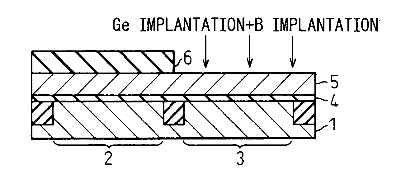
[0029] A silicon substrate 1 isolated in advance by shallow trench isolation (STI) to form an nMOS region 2 and a pMOS region 3 is formed with a gate insulating film 4 to a thickness of 1.5 nm, then has deposited on it a polycrystalline silicon film 5 for formation of gate electrodes to a thickness of 120 nm (FIG. 3A).

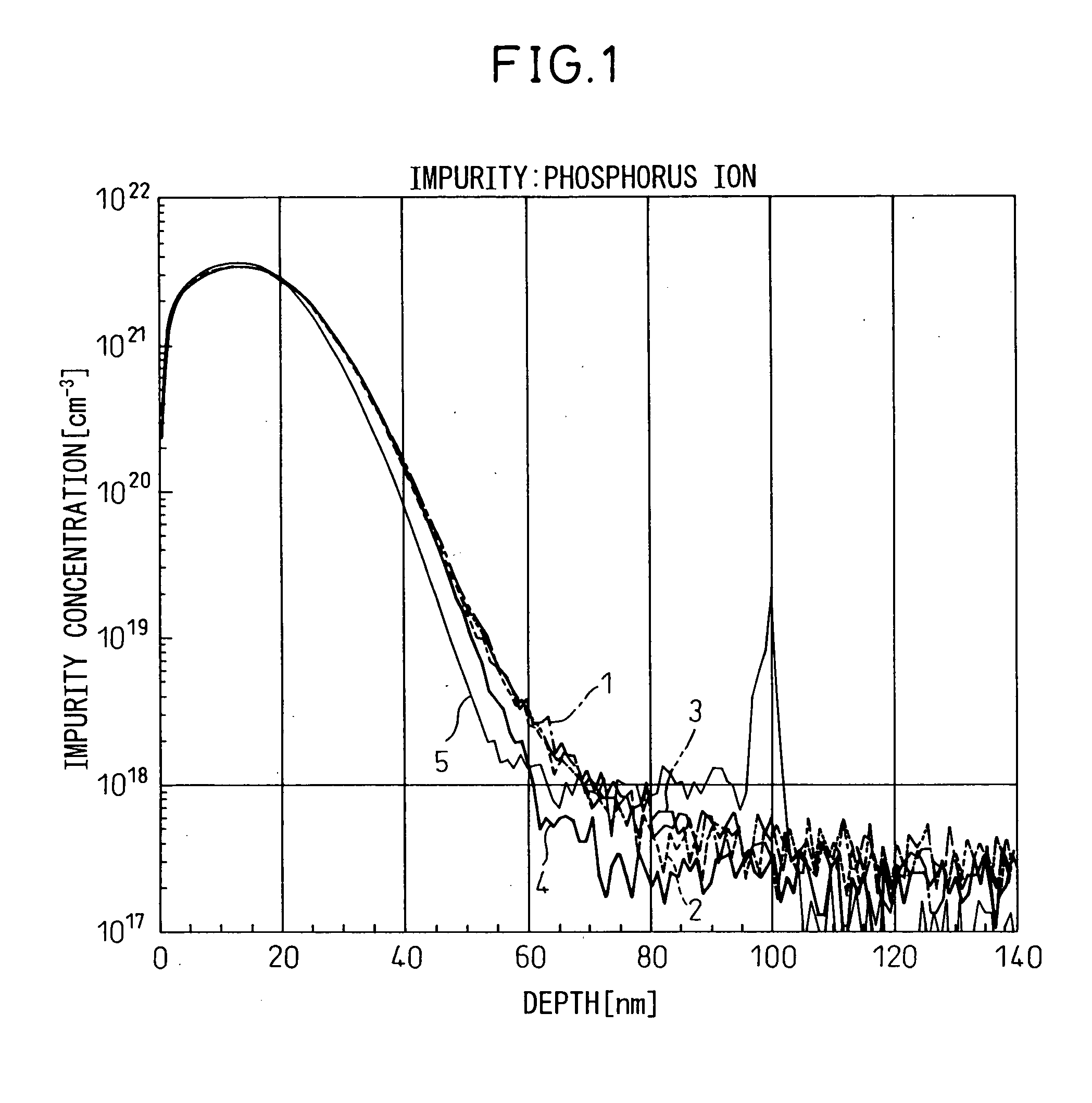
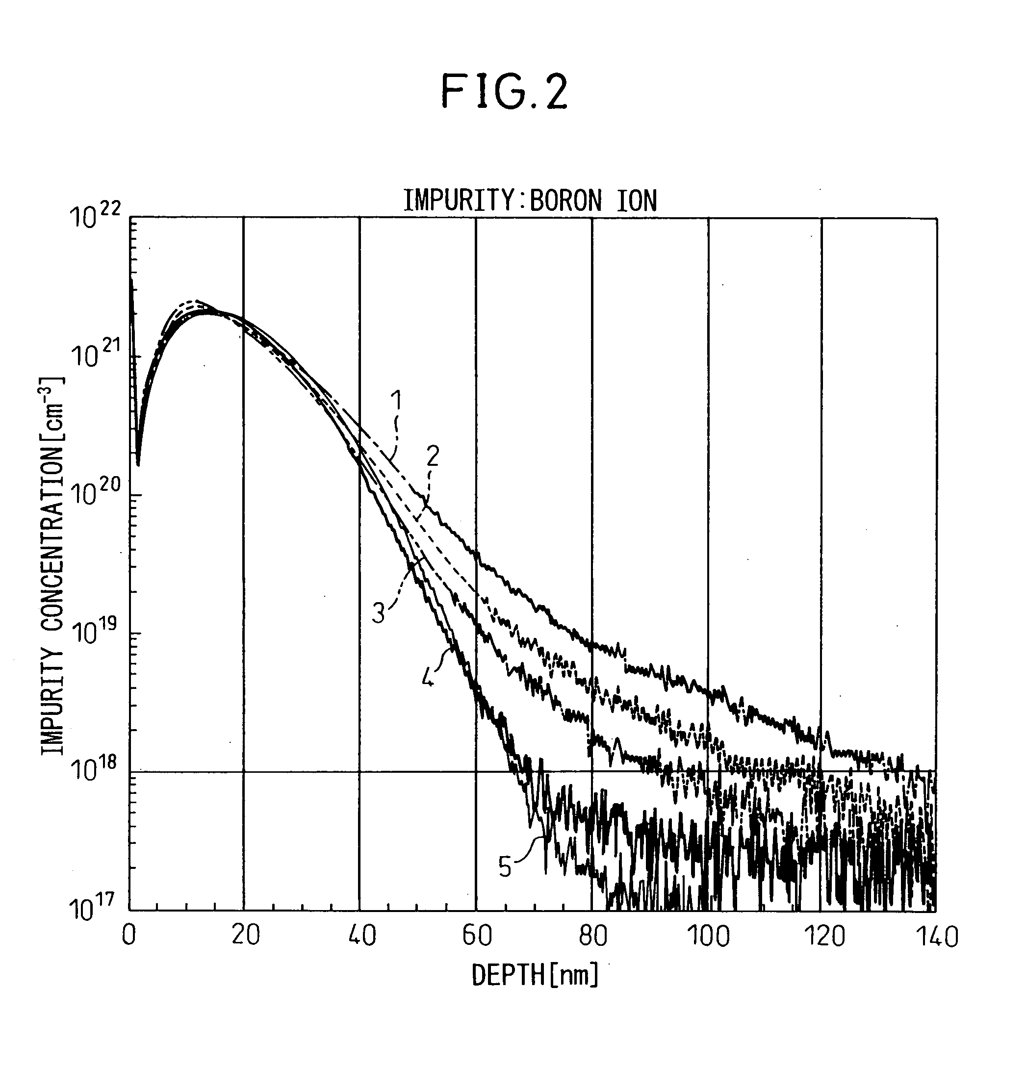
[0030] Next, a mask 6 is formed so as to enable an impurity to be introduced into the polycrystalline silicon film 5 at the nMOS region 2, then Ge is introduced by an energy of 20 keV and a dosage of 1.times.10.sup.15 / cm.sup.2 to preamorphize the polycrystalline silicon film 5. Next, phosphorus (P) ions are introduced by an energy of 10 keV and a dosage of 1.times.10.sup.15 / cm.sup.2 (FIG. 3B).

[0031] Next, the mask 6 is removed, then the gate is annealed in a rapid thermal annealing system (RTA) at 900.degree. C. for 30 seconds in an oxygen atmosp...

second embodiment

Production of CMOS Semiconductor Device by Predoping nMOS Region and pMOS Region

[0035] FIGS. 4A to 4G show the flow of steps for production of the present invention.

[0036] A silicon substrate 1 isolated in advance by shallow trench isolation (STI) to form an nMOS region 2 and a pMOS region 3 is formed with a gate insulating film 4 to a thickness of 1.5 nm, then has deposited on it a polycrystalline silicon film 5 for formation of gate electrodes to a thickness of 120 nm (FIG. 4A).

[0037] Next, a mask 6 is formed so as to enable an impurity to be introduced into the polycrystalline silicon film 5 at the nMOS region 2, then Ge is introduced by an energy of 20 keV and a dosage of 1.times.10.sup.15 / cm.sup.2 to preamorphize it. Next, phosphorus (P) ions are introduced by an energy of 10 keV and a dosage of 1.times.10.sup.15 / cm.sup.2 (FIG. 4B).

[0038] Next, the mask 6 is removed, then the gate is annealed in a rapid thermal annealing system (RTA) at 900.degree. C. for 30 seconds in an oxyge...


PUM

PropertyMeasurementUnit
temperatureaaaaaaaaaa
roughnessaaaaaaaaaa

Abstract

A method of manufacturing a CMOS semiconductor device able to reduce the effective thickness of the gate insulating film and able to secure stable performance is provided. The method in one embodiment comprises the steps of: forming a polycrystalline silicon film on a gate insulating film; introducing an n-type impurity into the polycrystalline silicon film in an nMOS formation region before gate processing of the polycrystalline silicon film; performing heat treatment so that the impurity diffuses in the polycrystalline silicon film and is activated; and patterning the polycrystalline silicon to form a gate pattern before introducing an impurity into the polycrystalline silicon film at a pMOS formation region.

Description

[0001] 1. Field of the Invention[0002] The present invention relates to a method of manufacturing a semiconductor device, more particularly relates to a method for manufacturing a CMOS semiconductor device which sufficiently activates an impurity introduced into a polycrystalline silicon gate electrode and reduces an effective thickness of the gate insulating film.[0003] 2. Description of the Related Art[0004] The increasing miniaturization of CMOS transistors has led to demand for a shallower junction between the source region and drain region. To obtain such a shallower junction, it is required that ions be implanted with a low energy and the activation annealing be performed at a lower temperature and in a shorter time than the past. When using polycrystalline silicon as a gate electrode, if annealing at a low temperature for a short time, the impurity implanted into the polycrystalline silicon gate electrode is not sufficiently activated. Therefore, the gate electrode becomes de...

Claims


Application Information

Patent Timeline
Patent Type & Authority Applications(United States)
IPC IPC(8): H01L21/28H01L21/8238H01L27/092H01L29/423H01L29/49
CPCH01L21/823842
Inventor KOJIMA, MANABUGOTO, KENICHIMORIOKA, HIROSHIOKABE, KENICHI
Owner FUJITSU SEMICON LTD
Why Eureka
Try Eureka