Image sensor having clamp circuit

Active Publication Date: 2004-08-12
INTELLECTUAL VENTURES II
View PDF18 Cites 40 Cited by
  • Summary
  • Abstract
  • Description
  • Claims
  • Application Information

AI Technical Summary

Benefits of technology

0018] It is, therefore, an object of the present invention to provide an image sensor for effectively reducing a dark

Problems solved by technology

Meanwhile, the image sensor has a fixed pattern noise generated by an offset voltage generated at a manufacturing process.
However, the conventional image sensor cannot naturally reproduce the bright object, e.g.

Method used


Image

  • Image sensor having clamp circuit
  • Image sensor having clamp circuit
  • Image sensor having clamp circuit

Examples


Embodiment Construction

[0027] In order to prevent a dark phenomenon that a bright object, e.g., a sun reflecting or emitting strong light, is rather darkly shown in an image frame, a voltage level of a reset voltage signal is maintained greater than or identical to a predetermined voltage level at the reading operation of the reset voltage signal.

[0028] Hereinafter, an image sensor using a correlated double sampling method (hereinafter, referred as CDS method) will be described in detail with reference to the accompanying drawings.

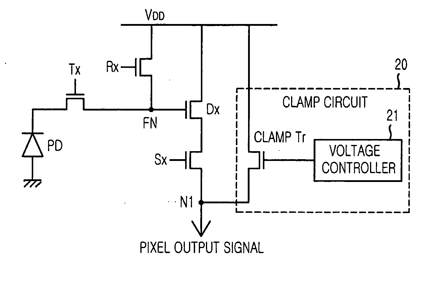
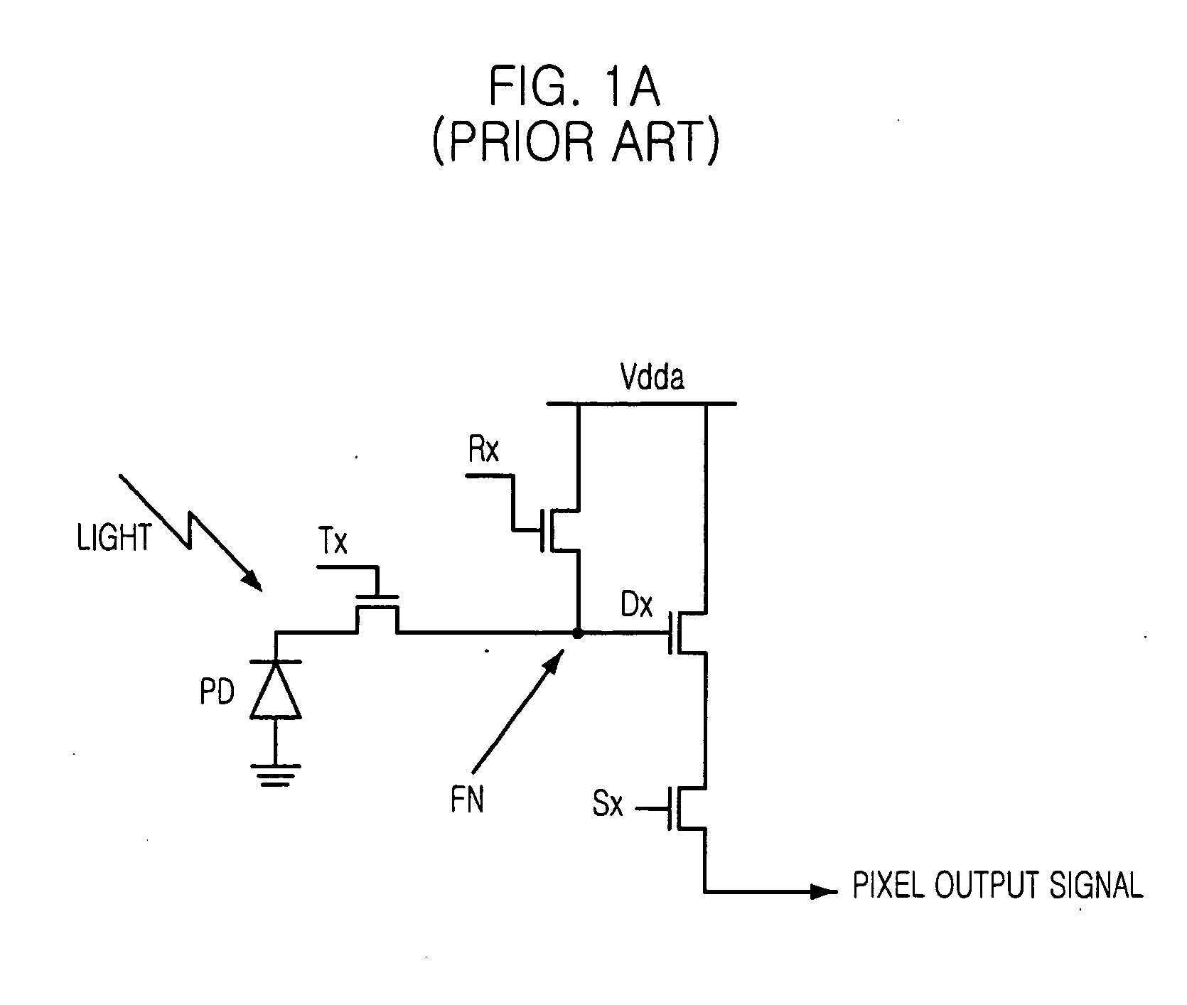
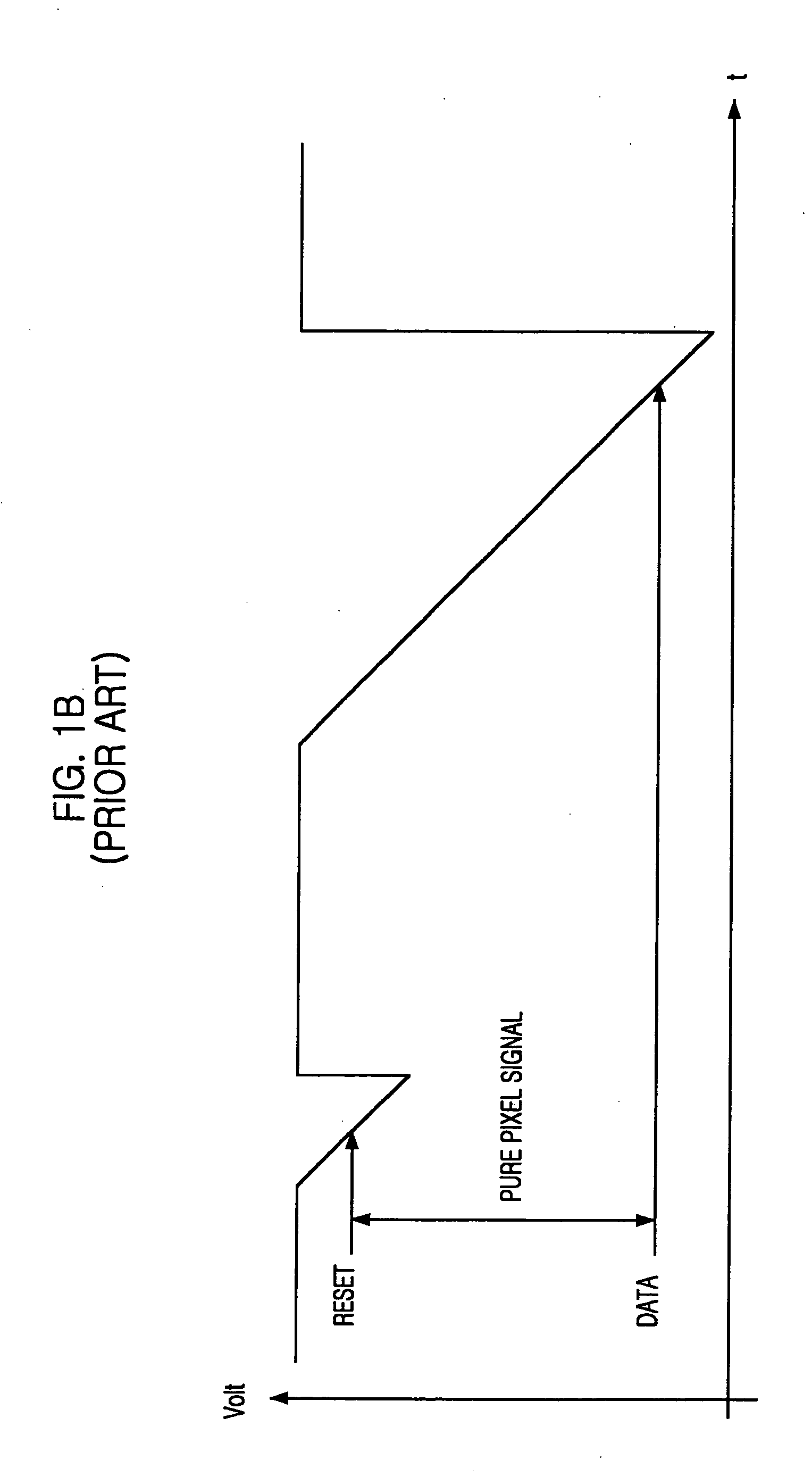
[0029] FIG. 2A is a schematic diagram depicting a unit pixel of an image sensor having a clamp circuit in accordance with an embodiment of the present invention. FIG. 2B is a graph describing a voltage level outputted from the unit pixel of the image sensor having the clamp circuit in accordance with the embodiment of the present invention in case of injecting a strong light into the unit pixel. Referring to FIG. 2, because the voltage level of the reset voltage signal is preven...


PUM


Abstract

An image sensor of the present invention prevents the phenomenon that surrounding background of a bright object reflecting or emitting strong light like the sun is presented at dark and improves image quality of the image sensor by controlling the brightness of the bright object. The image sensor using correlated double sampling technology which outputs data of an object by using difference between a reset voltage signal and a data voltage signal of a unit pixel includes a plurality of unit pixels arranged in a matrix, each outputting the reset voltage signal and the data voltage signal; a plurality of clamping means, each coupled to each unit pixels for clamping up the reset signal to a predetermined voltage level; and a voltage controlling block for adjusting voltage level supplied to a gate of each of clamping means.

Description

[0001] The present invention relates to an image sensor; and, more particularly, to the image sensor capable of preventing a phenomenon that an object, e.g., a light source like the sun becomes darker than a real image when strong light is inputted from the object.DESCRIPTION OF PRIOR ART[0002] An image sensor is a device for picking up light images by using a property, which causes a semiconductor to react to the light. Particularly, complementary metal oxide semiconductor (hereinafter, referred to a CMOS) devices are generally used in image sensors. A CMOS image sensor is designed by using a CMOS technology for designing a general control circuit or a signal processing circuit. In the CMOS image sensor, each pixel outputs electrical signals converted from optical values detected by each photodiode. Then, each MOS transistor connected to each pixel delivers the electrical signals to a signal processing unit.[0003] Meanwhile, the image sensor has a fixed pattern noise generated by a...

Claims


Application Information

Patent Timeline
IPC IPC(8): H04N5/335H01L27/146H04N5/357H04N5/363H04N5/378
CPCH04N5/3575H04N5/378H04N5/3598H04N25/616H04N25/627H04N25/75
Inventor BEA, CHANG-MINYOON, KWANG-HO
Owner INTELLECTUAL VENTURES II
Why Eureka
Try Eureka