Active matrix el display and its driving method

a technology of active matrix and display, applied in the direction of static indicating devices, instruments, electrical appliances, etc., can solve the problems of image quality deterioration and uneven display, and achieve the effect of accurate gradation display

Inactive Publication Date: 2004-10-07
JOLED INC
View PDF11 Cites 6 Cited by
  • Summary
  • Abstract
  • Description
  • Claims
  • Application Information

AI Technical Summary

Benefits of technology

0007] In view of the above-described problems, an object of the present invention is to provide an active matrix EL displa...

Problems solved by technology

However, in a transistor formed with a low-temperature polysilicon that can be formed on an inexpensive glass substrate, the threshold value has a variation in a range of .+-.0.2 V to 0.5 V. As a result, the ON current flowing in the driving transistor 104 varies corresponding thereto, resulting in uneven...

Method used


Image

  • Active matrix el display and its driving method
  • Active matrix el display and its driving method
  • Active matrix el display and its driving method

Examples


first embodiment

[0037] (First Embodiment)

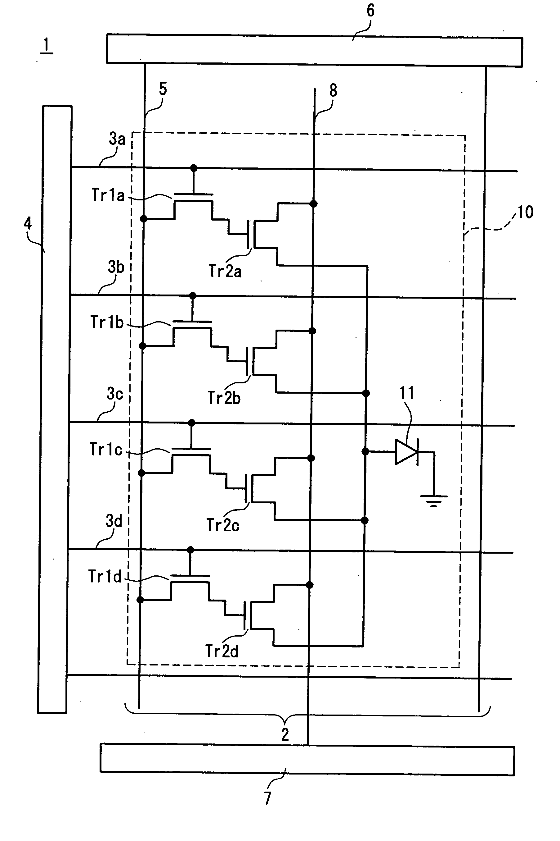
[0038] FIG. 1 shows a circuit structure of an active matrix EL display device, according to a first embodiment of the present invention. This EL display device 1 is based on a digital driving system for providing a gradation display by means of a digital image signal. The digital image signal is composed of 4 bit data, and it can provide 16level gradation display.

[0039] A display portion 2 of the EL display device 1 is composed by arraying a plurality of unit pixels 10. Though plural unit pixels 10 are arrayed in a matrix in an actual device, only one unit pixel 10 is shown in FIG. 1 for the sake of clarity. Each unit pixel 10 has a single EL element 11 functioning as a light-emitter. Four driving transistors Tr2a-Tr2d as current controlling elements are arranged in each of the unit pixels 10, and either the source electrodes or the drain electrodes are connected to a pixel electrode composing the EL element 11. Either source electrodes or drain electrodes o...

second embodiment

[0061] (Second Embodiment)

[0062] FIG. 6 shows a circuit structure of a unit pixel 10a of an active matrix EL display device la according to a second embodiment. Components that are the same as those of the EL display device shown in FIG. 1 are provided with identical reference numbers, and the description will not be repeated.

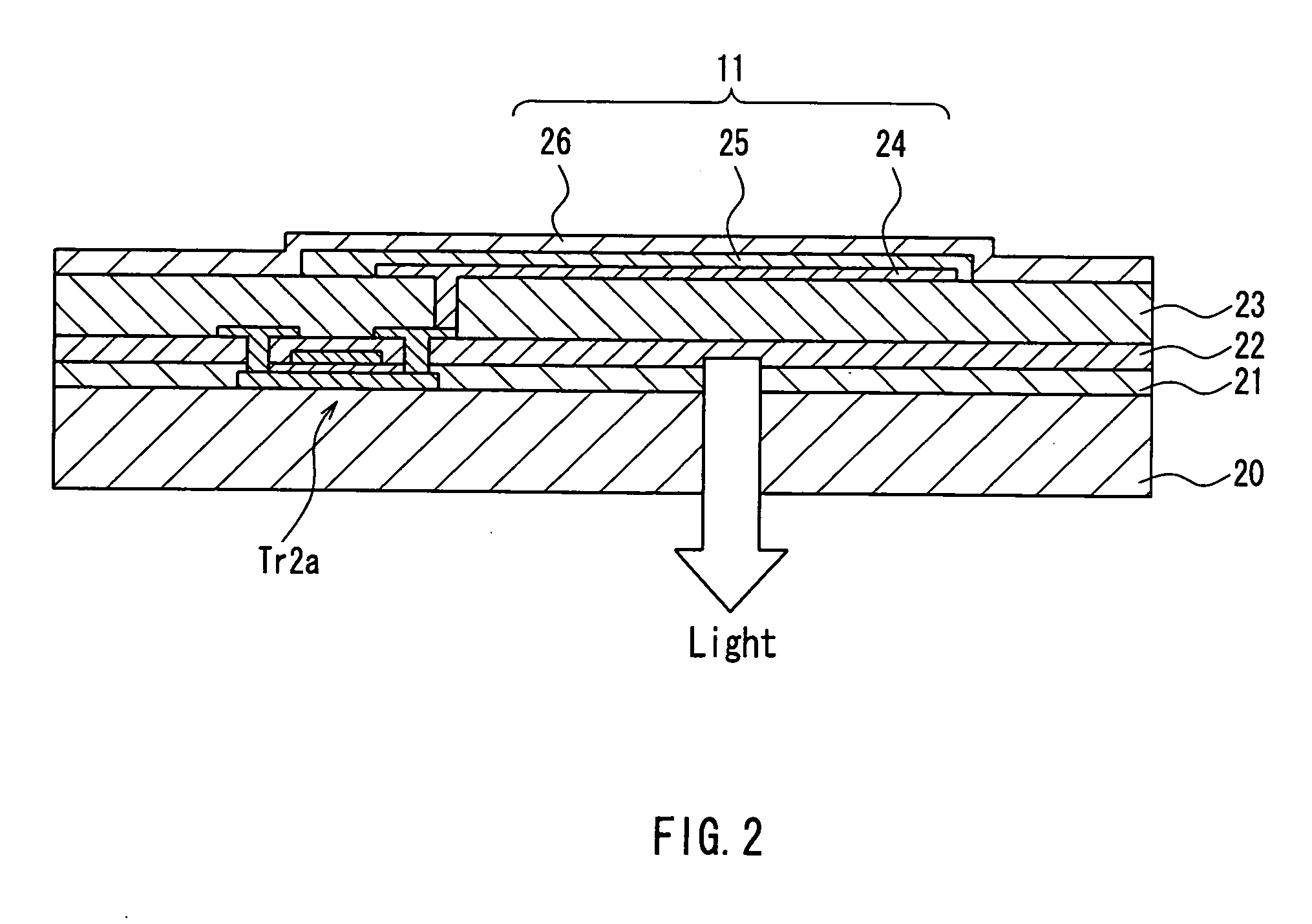
[0063] In the second embodiment, both the switching transistors Tr1a-Tr1d and the driving transistors Tr2a-Tr2d are N-channel type transistors. A schematic structure of an EL element 11a and a driving transistor Tr2a is shown in FIG. 7. A pixel electrode 24a is a cathodic electrode of the EL element 11a, and a counter electrode 26a is an anodic electrode. The pixel electrode 24a as a cathodic electrode is an opaque electrode, while the counter electrode 26a as an anodic electrode is an ITO electrode. Excepting these, the configuration is identical to that of FIG. 1. In this configuration, light of the EL light-emitting layer 25 is irradiated from the direction ...

third embodiment

[0066] (Third Embodiment)

[0067] FIG. 8 shows a circuit structure of a unit pixel 10b of an active matrix EL display device 1b according to a third embodiment. Components that are the same as those of the EL display device shown in FIG. 1 are provided with identical reference numbers, and the description will not be repeated.

[0068] In this embodiment, an auxiliary capacitor 12 is provided between each of driving transistors Tr2a-Tr2d and each of scanning lines 3b-3e in the succeeding column. By providing the auxiliary capacitors 12, fluctuations in the gate voltages of the driving transistors Tr2a-Tr2d can be reduced. For example, when leakage current at the time that the switching transistors Tr1a-Tr1d are OFF is large, the gate voltages of the driving transistors Tr2a-Tr2d may vary. The auxiliary capacitors 12 are especially effective for such a case. The auxiliary capacitors 12 can have a common capacitance, or the capacitances can be set to a ratio corresponding to a ratio in the...


PUM


Abstract

A unit pixel (10) includes a plurality of current controlling elements (Tr2a-Tr2d) having controlling terminal and connected to a single EL element (11), and switching elements (Tr1a-Tr1d) provided to the respective current controlling elements in order to switch between application and cutoff of a digital image signal with respect to the controlling terminals in accordance with the condition of a scanning signal. Each of the current controlling elements is controlled by a voltage of the digital image signal so as to take an OFF state for cutting off a supply of a driving current to the EL element or an ON state for supplying the EL element with a driving current corresponding to the voltage of the digital image signal, and a value of the current flowing in the EL element is the sum value of currents supplied from the respective current controlling elements in the ON state. Based on a combination of the current controlling elements in the ON state, the current supplied to the EL element is controlled to be a value corresponding to the gradation.

Description

[0001] The present invention relates to an active matrix EL display device used in so-called portable equipment or the like, and a method of driving the device.[0002] FIG. 12 shows a configuration of a conventionally-typical active matrix EL display device 101. The numeral 102 denotes a unit pixel contained in the active matrix EL display device 101. Though unit pixels 102 are arrayed in a matrix in an actual device, only one unit pixel is shown here for the sake of clarity. The unit pixel 102 includes an EL element 103, a driving transistor 104 connected to one end of the EL element 103, a switching transistor 105 connected to a gate of the driving transistor 104, and a capacitor 106. To a gate of the switching transistor 105, a scanning signal is supplied from a scanning-driving circuit 108 through a scanning line 107. To the gate of the driving transistor 104, an image signal is supplied from a signal-driving circuit 110 via the switching transistor 105 and a signal line 109. To ...

Claims


Application Information

Patent Timeline
IPC IPC(8): G09G3/32
CPCG09G3/3233G09G3/3258G09G2300/0417G09G2300/0426G09G2300/0465G09G2300/0828G09G2300/0842
Inventor SENDA, KOUJINANNO, YUTAKATSUTSU, HIROSHI
Owner JOLED INC
Why Eureka
Try Eureka