Semiconductor integrated circuit and test method thereof

Inactive Publication Date: 2004-10-14
SOCIONEXT INC
View PDF3 Cites 8 Cited by
  • Summary
  • Abstract
  • Description
  • Claims
  • Application Information

AI Technical Summary

Problems solved by technology

Therefore, in order to achieve the repair processes for the memory and the scan test for the BIST, the memory element for repai

Method used


Image

  • Semiconductor integrated circuit and test method thereof
  • Semiconductor integrated circuit and test method thereof
  • Semiconductor integrated circuit and test method thereof

Examples


first embodiment

[0070] (First Embodiment)

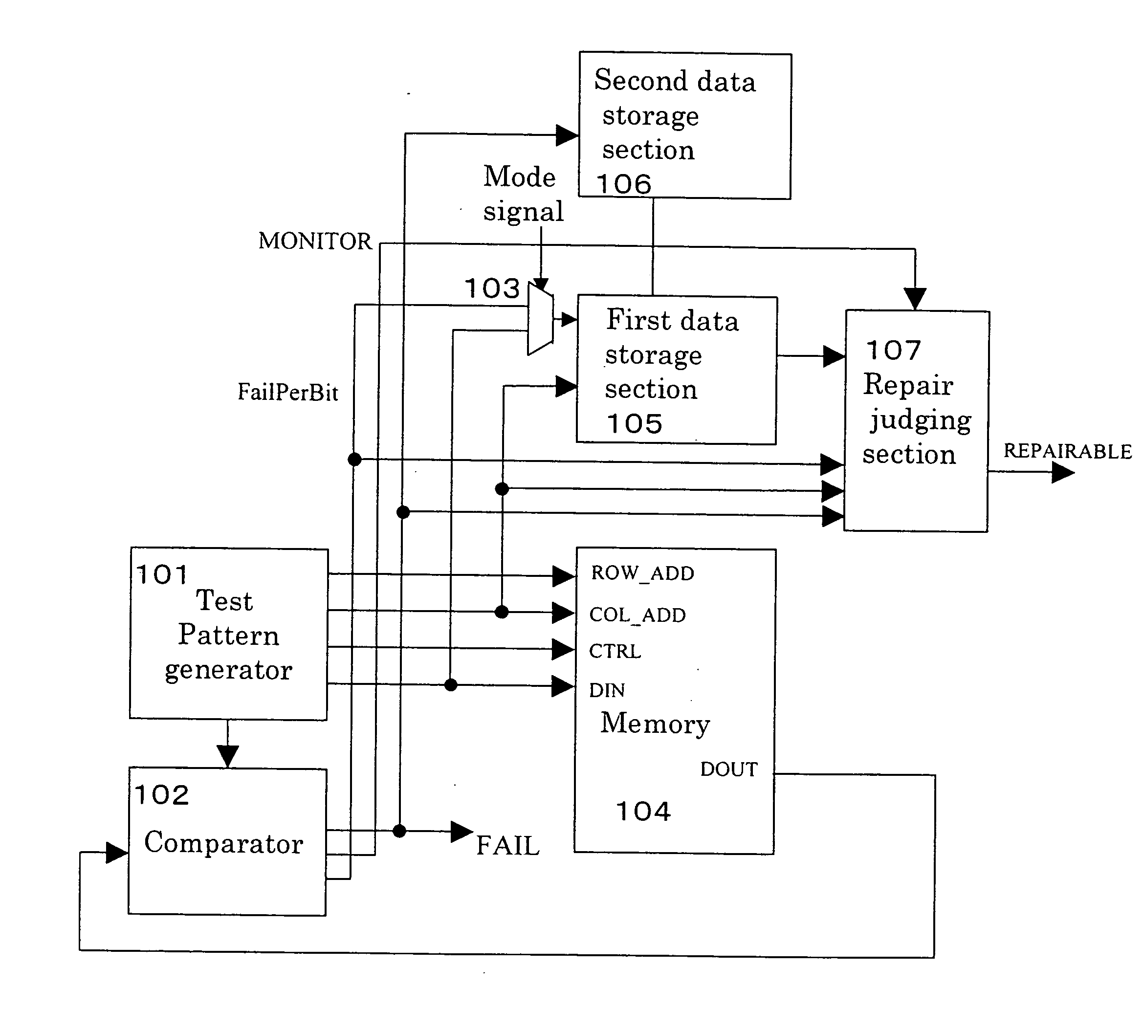
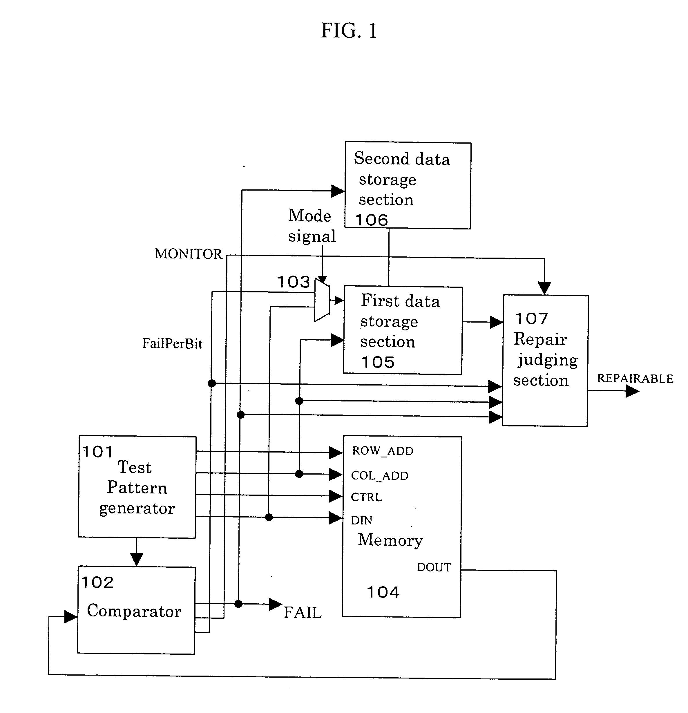
[0071] FIG. 1 is a block diagram for describing a semiconductor integrated circuit according to a first embodiment of the present invention.

[0072] A memory 104 represents a memory to be tested, which has a set of redundant lines for repair in a Column direction, and in the embodiment, includes a single Column line for repair which is replaced by the repair processes therein.

[0073] Symbol 101 represents a test pattern generating section, which generates a Row address signal ROW_ADD, a Column address signal COL_ADD, a control signal CTRL, and a data input signal DIN, and inputs them into the memory 104.

[0074] Symbol 102 represents a comparing section, which compares an output response DOUT of the memory 104 with respect to the test pattern inputted into the memory 104 with a value expected when the memory is normal (expected value), and detects a faulty cell which does not normally store the signal. The comparing section 102 generates a FAIL signal which becom...

second embodiment

[0122] (Second embodiment)

[0123] FIG. 6 is a block diagram for describing a semiconductor integrated circuit according to a second embodiment of the present invention.

[0124] A memory 604 represents a memory to be tested, which has a set of redundant lines for repair in the Row direction, and in the embodiment, includes a single Row line for repair which is replaced by the repair processes therein.

[0125] Symbol 601 represents a test pattern generating section, which generates a Row address signal ROW_ADD, a Column address signal COL_ADD, a control signal CTRL, and a data input signal DIN, and inputs them into the memory 604.

[0126] Symbol 602 represents a comparing section, which compares an output response DOUT of the memory 604 with respect to the test pattern inputted into the memory 604 with a value expected when the memory is normal (expected value), and detects a faulty cell which does not normally store the signal. The comparing section 602 generates a FAIL signal which becomes...

third embodiment

[0169] (Third Embodiment)

[0170] FIG. 10 is a block diagram for describing a semiconductor integrated circuit according to a third embodiment of the present invention.

[0171] A memory 1004 represents a memory to be tested, which has redundant lines for repair in a Column direction and a Row direction, and in the embodiment, includes a single Column line for repair and a single Row line for repair which are replaced by the repair processes therein.

[0172] Symbol 1001 represents a test pattern generating section, which generates a Row address signal ROW_ADD, a Column address signal COL_ADD, a control signal CTRL, and a data input signal DIN, and inputs them into the memory 1004.

[0173] Symbol 1002 represents a comparing section, which compares an output response DOUT of the memory 1004 with respect to the test pattern inputted into the memory 1004 with a value expected when the memory is normal (expected value), and detects a faulty cell which does not normally store the signal. The compa...


PUM


Abstract

In order to achieve a redundant repair for a memory using a BIST, a semiconductor integrated circuit which can suppress an increase in circuit area for redundant repair and circuit area for scan test, and an test method thereof are provided. It comprises: a memory 104, which has a redundant line for repair in a Column direction; a test pattern generating section 101; a comparing section 102, which judges whether a faulty cell exists in the memory 104 or not, a first data storage section 105, which during an test of the memory 104, retrieves a signal inputted into the memory 104 from the test pattern generating section 101 and a pass/fail judgment signal for every bit from the comparing section 102, and during an test of a peripheral logic of the memory, is used for observing an input signal into the memory 104; a second data storage section 106, which shows a state of the presence or absence of a failure; and a repair judging section 107, wherein data of the first data storage section 105 is held by the second data storage section 106.

Description

[0001] 1. Field of the Invention[0002] The present invention relates to a semiconductor integrated circuit capable of testing a memory, in particular testing a memory having a redundant cell and testing a peripheral logic of the memory, using a Built In Self Test (BIST), and an test method thereof.[0003] 2. Description of the Prior Art[0004] Recently, the number and the scale of the memories (bit width and the number of words), which have been mounted in a semiconductor integrated circuit (LSI), have been increased. According to this, the number of external pins and the test time which are needed for inspecting the memory mounted in the LSI using a circuit tester from the outside increase.[0005] In contrast to this, importance of a BIST (Built In Self Test, hereinafter referred to as BIST) technology for executing the test of the memory within the LSI has been increased. By using the BIST technology, while being able to inspect the memory using fewer external pins, it becomes possib...

Claims


Application Information

Patent Timeline
IPC IPC(8): G11C29/12G01R31/28G11C29/44
CPCG11C29/44G11C29/4401G11C2029/0405G11C2029/1208
Inventor ICHIKAWA, OSAMU
Owner SOCIONEXT INC
Why Eureka
Try Eureka