Electro-optical device, method of manufacturing the same, and electronic apparatus

a technology of optical devices and electronic devices, applied in the direction of identification means, instruments, tube shearing machines, etc., can solve the problems of affecting the operation of the device, the underlying light-emitting layer, or the like, deterioration, and substantially high reactivity

Active Publication Date: 2004-10-28
SEIKO EPSON CORP
View PDF10 Cites 100 Cited by
  • Summary
  • Abstract
  • Description
  • Claims
  • Application Information

AI Technical Summary

Problems solved by technology

However, as a display becomes larger, thin and lightweight, panel structure requires a shift from a hollow structure to a solid structure to have strength resistant to external stress.
However, there is a problem that an underlying light-emitting layer, or the like, is deteriorated under the influence of ultraviolet or plasma ions generated upon forming the film.
Moreover, it is required to protect the light-emitting element or the like from such ultraviolet since the ultraviolet contained in an outer light degrades a life span of the element even upon using such an electro-optical device at outdoors places as well as during manufacturing steps.
In particular, in case of an element, such as an EL light-emitting element, that performs its function when a carrier, supplied from the first electrode or the second electrode, passes through the electro-optical layer, at least some parts of the element may have different properties, such that electrons and holes, and charge balance may be disturbed.
These portions have substantially high reactivity and generate structural defects (i.e., capture site of the carrier) by reacting with, for example, oxygen, water or the like, which causes a function degradation of the electro-optical lay

Method used


Image

  • Electro-optical device, method of manufacturing the same, and electronic apparatus
  • Electro-optical device, method of manufacturing the same, and electronic apparatus
  • Electro-optical device, method of manufacturing the same, and electronic apparatus

Examples


first exemplary embodiment

[0048] First Exemplary Embodiment

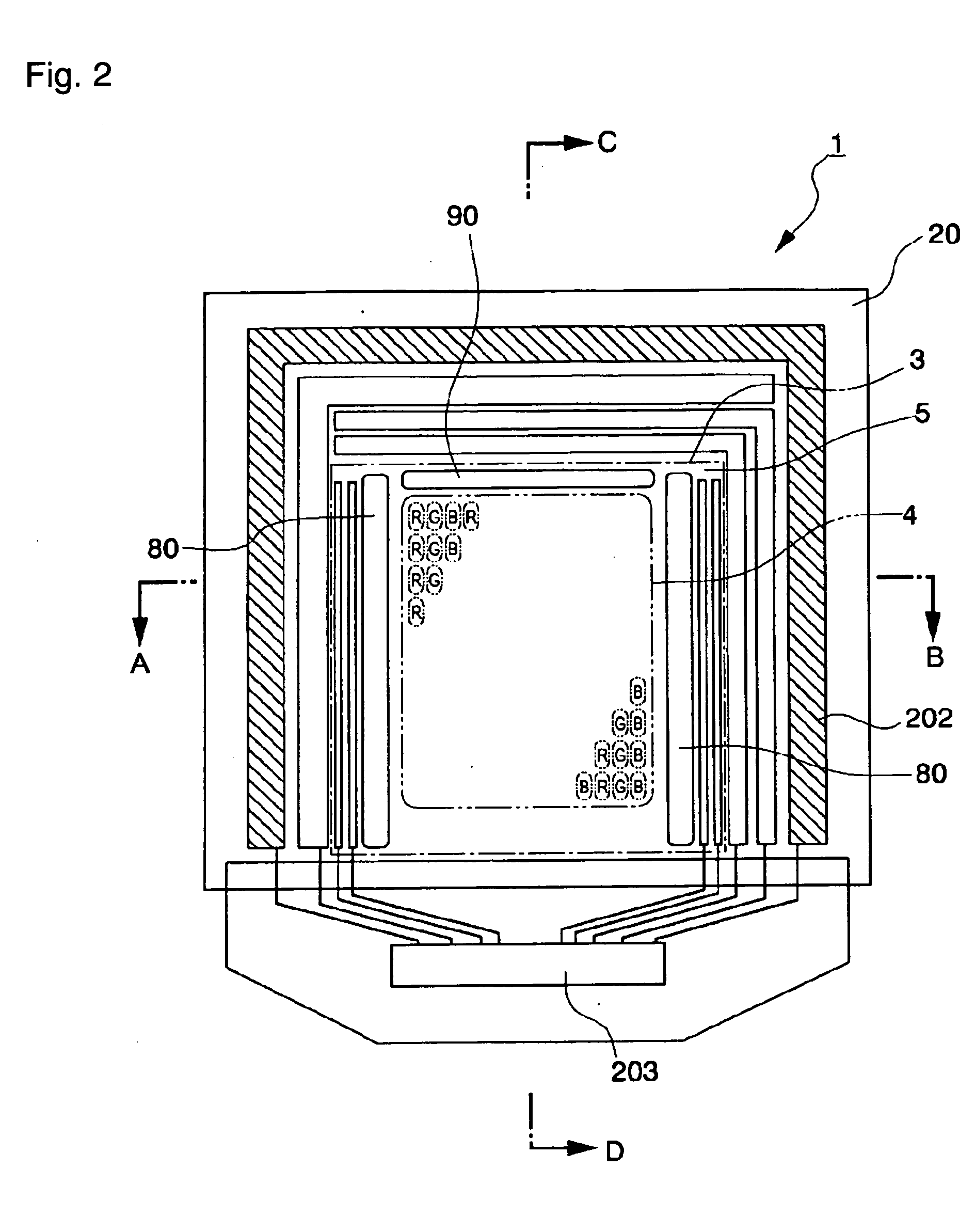
[0049] An electro-optical device according to a first exemplary embodiment of the present invention will be described with reference to FIGS. 1 to 10.

[0050] First of all, an EL display device using an organic electroluminescent (EL) material as an example of an electro-optical device to which a manufacturing method of an aspect of the present invention is applied will be described prior to describing a method of manufacturing an electro-optical device of an aspect of the present invention.

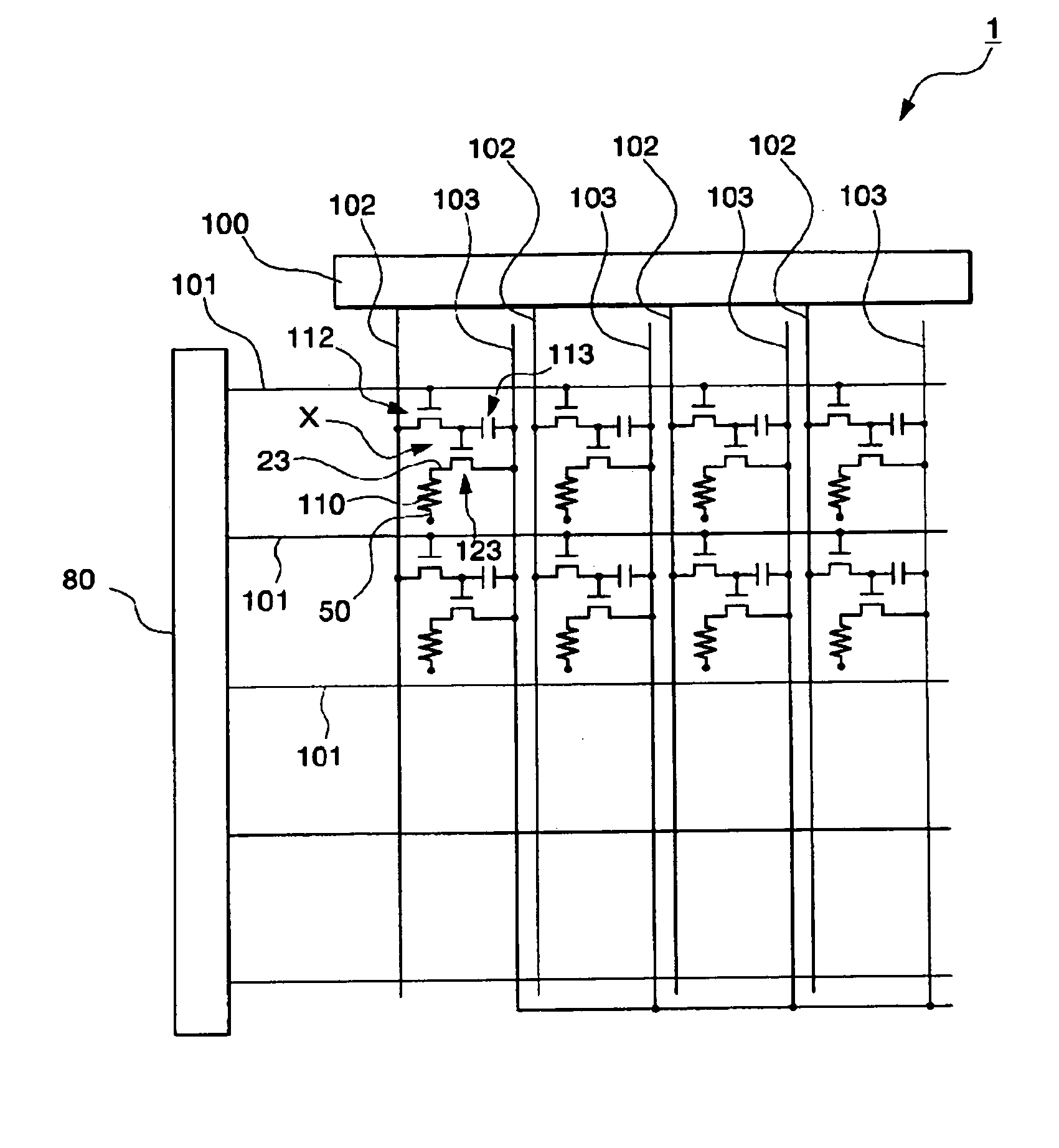
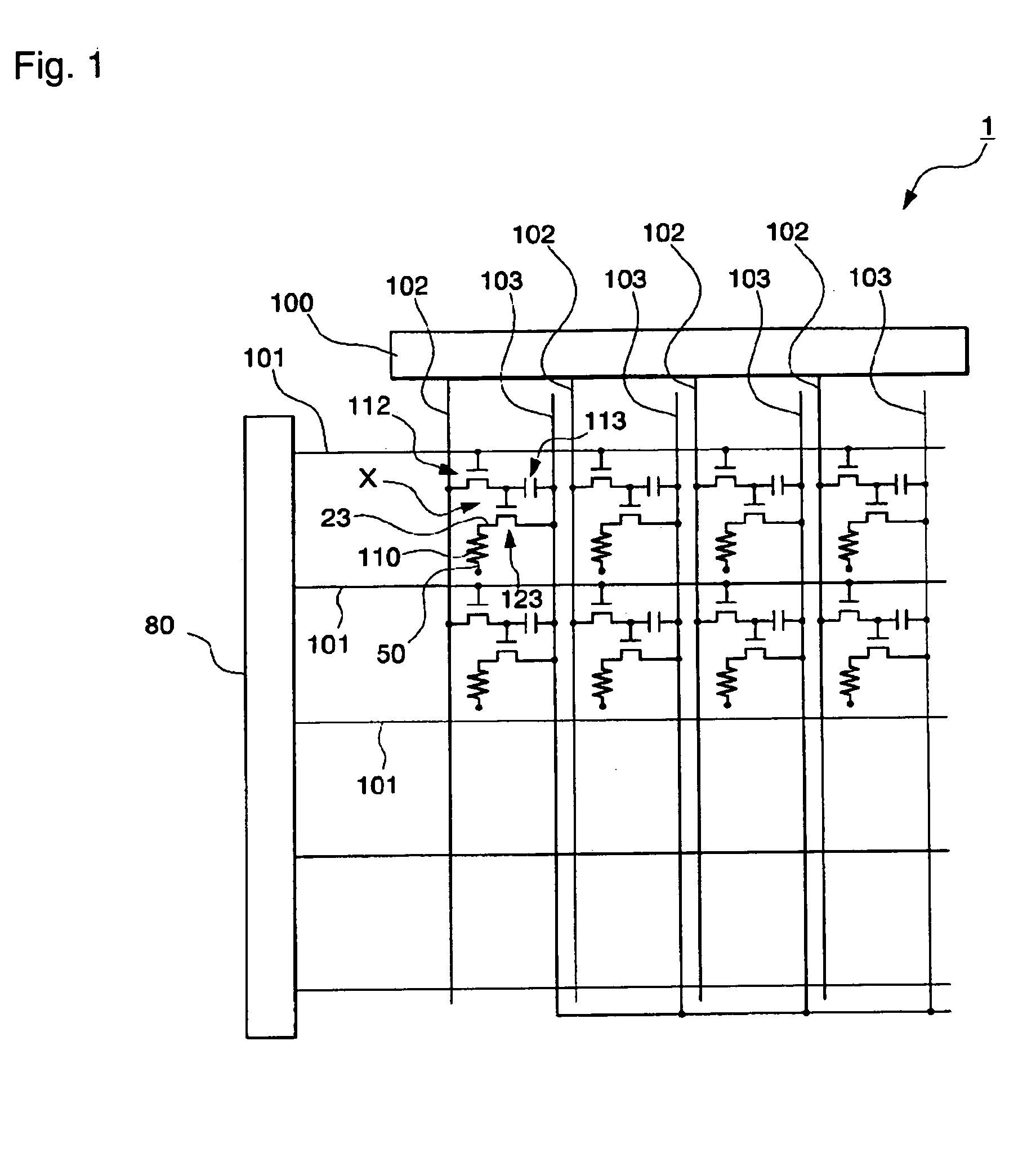
[0051] A wiring structure of the EL display device in this example will be described with reference to FIG. 1.

[0052] The EL display device (i.e., electro-optical device) 1 shown in FIG. 1 is an active matrix type EL display device using a thin film transistor (hereinafter, "TFT") as a switching element.

[0053] This EL display device 1, as shown in FIG. 1, includes a plurality of scan lines 101, a plurality of signal lines 102 extended in a crossing direction perpendi...

second exemplary embodiment

[0136] Second Exemplary Embodiment

[0137] Next, an electro-optical device according to a second exemplary embodiment of the present invention will be described with reference to FIG. 11.

[0138] This exemplary embodiment enhances insulating property between the ultraviolet absorbing layer and the cathode by making nitrogen to be included in the interface at the side of the cathode 50 of the ultraviolet absorbing layer in the configuration of the first exemplary embodiment.

[0139] An ultraviolet absorbing layer 30' provided to cover the cathode 50 in an electro-optical device 1' is formed of a laminated film of a first absorption layer 30a and a second absorption layer 30b. A barrier layer 40 is provided on the second absorption layer 30b.

[0140] Specifically, the first absorption layer 30a, contiguous with the cathode 50, and the second absorption layer 30b, contiguous with the gas barrier layer 40, are formed of TiON (oxynitride titanium) and TiO.sub.2, respectively. Since addition of n...

third exemplary embodiment

[0144] Third Exemplary Embodiment

[0145] Next, an electro-optical device according to a third exemplary embodiment of the present invention will be described with reference to FIG. 12.

[0146] In this exemplary embodiment, the outer side of the gas barrier layer 40 of the first exemplary embodiment is sealed by the protecting layer 204. That is, in this exemplary embodiment, the protecting layer 204 is provided on the base body 200 to cover the gas barrier layer 40. This protecting layer 204 is composed of an adhesive layer 205 provided in the gas barrier layer 40 and a protective substrate 206 disposed thereon.

[0147] The adhesive layer 205 has a function to adhere to the gas barrier layer 40 and to buffer mechanical shock from the exterior. For example, the adhesive layer 205 is formed of an adhesive composed of a urethane, acryl, epoxy, polyolefin, or siliconresin or the like, which is more flexible and has a lower glass transition point than the material of the protective substrate ...


PUM

PropertyMeasurementUnit
Thicknessaaaaaaaaaa
Angleaaaaaaaaaa
Band gapaaaaaaaaaa

Abstract

A method of manufacturing an electro-optical device, the electro-optical device having an electro-optical element formed by laminating a first electrode, an electro-optical layer, and a second electrode in sequence on a base body, the method of manufacturing the electro-optical device, including the steps of: forming an ultraviolet absorbing layer on the substrate by a vapor deposition method so as to cover the electro-optical element; and forming a gas barrier layer by a vapor deposition method using plasma so as to cover the ultraviolet absorbing layer.

Description

[0001] 1. Field of Invention[0002] The present invention relates to an electro-optical device, a method of manufacturing the same, and an electronic apparatus including the electro-optical device.[0003] 2. Description of Related Art[0004] In the field of electro-optical devices, there is a need for durability enhancement against oxygen, moisture, or the like. For example, an organic EL element constituting an organic EL display is formed from an inorganic anode, (an organic hole injecting layer), an organic light-emitting layer, (an electron injecting layer) and inorganic cathode. Particularly, the electron injecting layer having a material property of easy electron emission reacts easily with moisture present in atmosphere. As a result of reacting with water, the electron injection effect is diminished and a non-light-emitting region called dark spot may be formed.[0005] Therefore, there is a need for a sealing structure to block moisture. In the related art, a structure has been u...

Claims


Application Information

Patent Timeline
IPC IPC(8): G02F1/1333G02F1/1368G09F9/00G09F9/30H01L27/32H01L51/52H05B33/04H05B33/10H05B33/12H05B33/22
CPCH01L27/3295H01L51/5237H01L2251/5315H10K59/122H10K50/822H10K2102/3026H10K50/844H10K2101/30B23D21/04B23D35/001B23D33/02
Inventor HAYASHI, KENJI
Owner SEIKO EPSON CORP
Why Eureka
Try Eureka