CMOS imaging for ALC and CDS

a technology of alc and cds, applied in the field of imaging devices, can solve the problem that alc is not readily used with a conventional 4t pixel cell, and achieve the effect of improving the image quality and reducing the cost of operation

Active Publication Date: 2005-01-06
APTINA IMAGING CORP
View PDF10 Cites 39 Cited by
  • Summary
  • Abstract
  • Description
  • Claims
  • Application Information

AI Technical Summary

Benefits of technology

[0013] Embodiments of the invention provide pixel cells and methods of forming pixel cells that include two photo-conversion devices. Separate outpu

Problems solved by technology

Therefore, ALC is not readily used

Method used


Image

  • CMOS imaging for ALC and CDS
  • CMOS imaging for ALC and CDS
  • CMOS imaging for ALC and CDS

Examples


Embodiment Construction

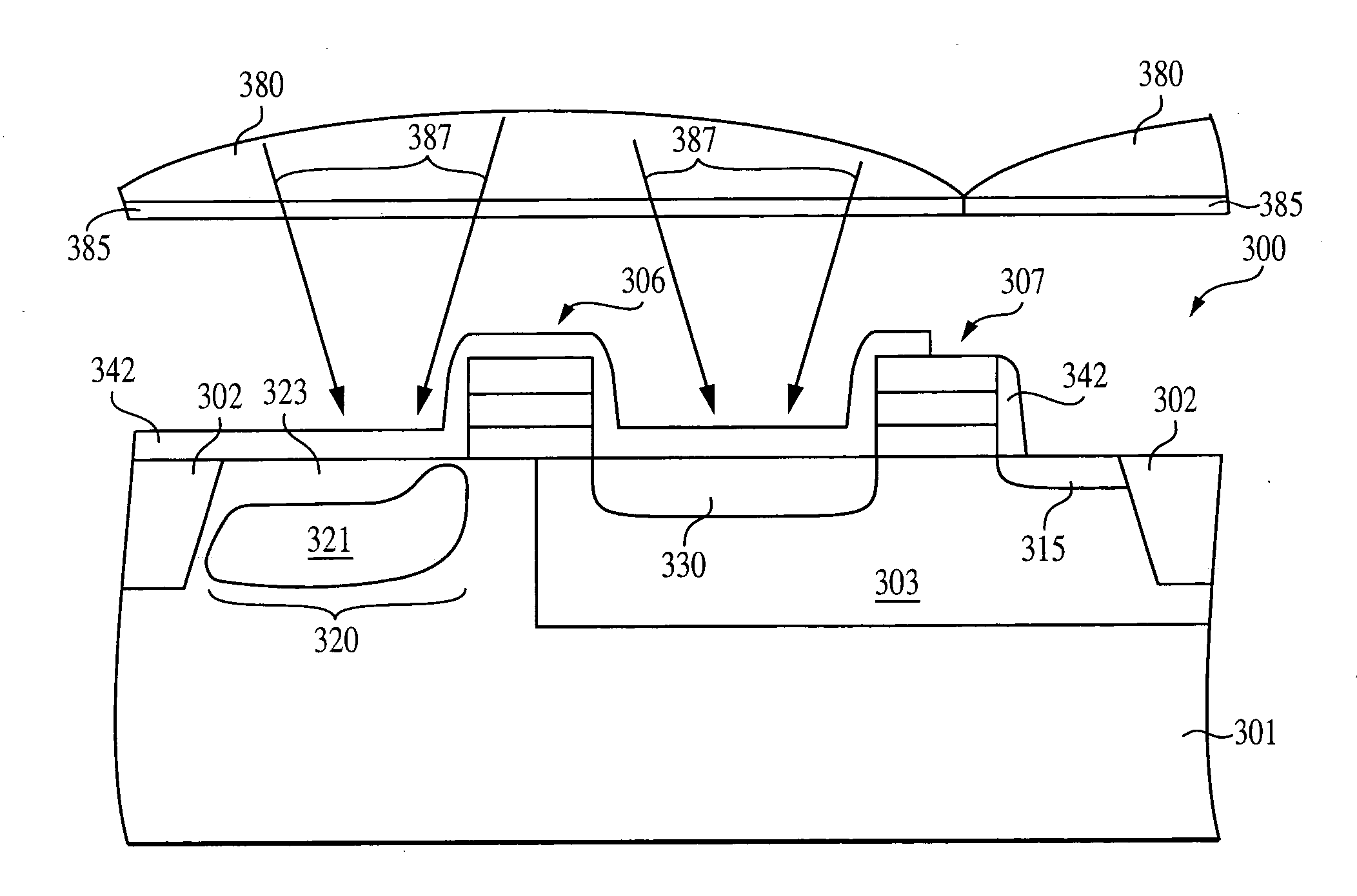
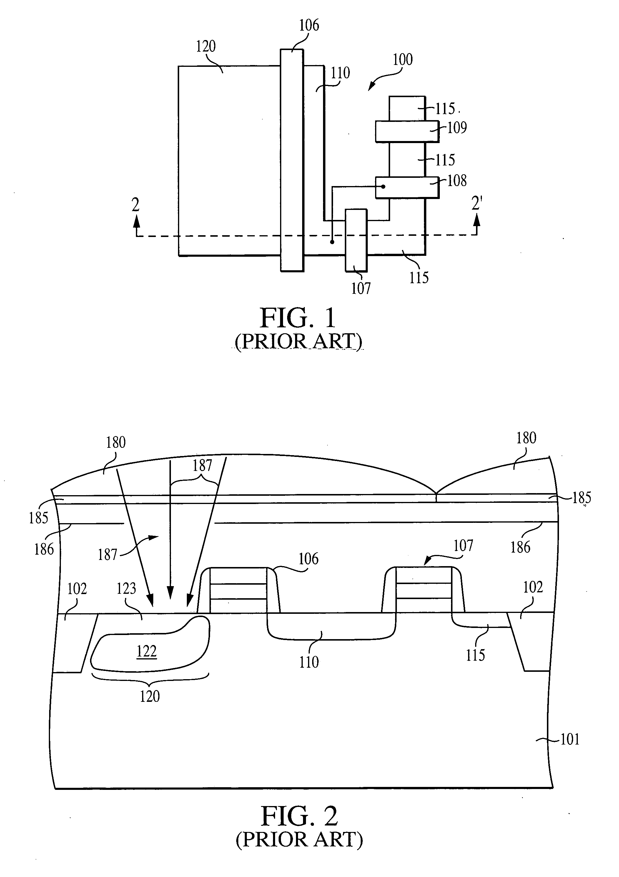
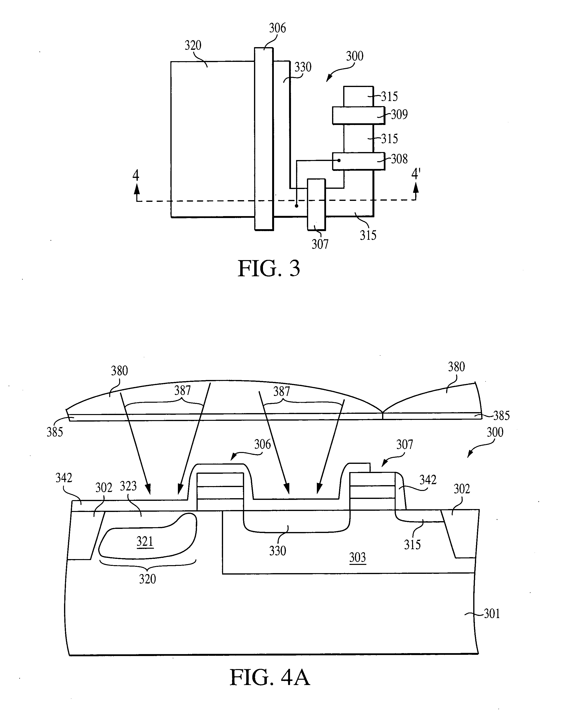
[0039] In the following detailed description, reference is made to the accompanying drawings, which form a part hereof and illustrate specific embodiments in which the invention may be practiced. In the drawings, like reference numerals describe substantially similar components throughout the several views. These embodiments are described in sufficient detail to enable those skilled in the art to practice the invention, and it is to be understood that other embodiments may be utilized, and that structural, logical and electrical changes may be made without departing from the spirit and scope of the present invention.

[0040] The terms “wafer” and “substrate” are to be understood as including silicon, silicon-on-insulator (SOI), or silicon-on-sapphire (SOS) technology, doped and undoped semiconductors, epitaxial layers of silicon supported by a base semiconductor foundation, and other semiconductor structures, as well as insulating substrates such as glass or quartz. Furthermore, when...


PUM


Abstract

Embodiments of the invention provide pixel cells that allow both automatic light control and correlated double sampling operations. The pixel cell includes first and second photo-conversion devices that can be separately read out. For example, the second photo-conversion device can be the pixel cells' floating diffusion region, with an area and doping profile suitable for photo-conversion. An image sensor may include an array of pixel cells, some or all of which have two photo-conversion devices, and peripheral circuitry for reading out signals from the pixel cells. The image sensor's readout circuitry may monitor charge generated by the second photo-conversion devices to determine when to read out signals from the first photo-conversion devices.

Description

CROSS REFERENCE TO OTHER APPLICATION [0001] This patent application claims the benefit of U.S. provisional patent application Ser. No. 60 / 483,906, filed Jul. 2, 2003, entitled CMOS IMAGING FOR ALC AND CDS. U.S. provisional patent application Ser. No. 60 / 483,906 is hereby incorporated by reference in its entirety.FIELD OF THE INVENTION [0002] The present invention relates to the field of imaging devices, particularly to improved pixel cells capable of supporting automatic light control and correlated double sampling operations. BACKGROUND OF THE INVENTION [0003] A typical conventional CMOS imager circuit includes a focal plane array of pixel cells. Each cell includes a photo-conversion device such as, for example, a photogate, photoconductor, or photodiode, for generating and accumulating photo-generated charge in a portion of the substrate of the array. A readout circuit connected to each pixel cell includes at least an output transistor, which receives photo-generated charges from ...

Claims


Application Information

Patent Timeline
IPC IPC(8): H01L27/148H04N3/15
CPCH01L27/1462H01L27/14627H04N3/155H01L27/14887H01L27/14806H04N25/533H04N25/778H04N25/76H04N25/75
Inventor RHODES, HOWARD E.
Owner APTINA IMAGING CORP
Why Eureka
Try Eureka