

Method of manufacturing semiconductor device and method of manufacturing electronics device
- Summary
- Abstract
- Description
- Claims
- Application Information
AI Technical Summary
Benefits of technology
Problems solved by technology
Method used
Image

Examples
first embodiment
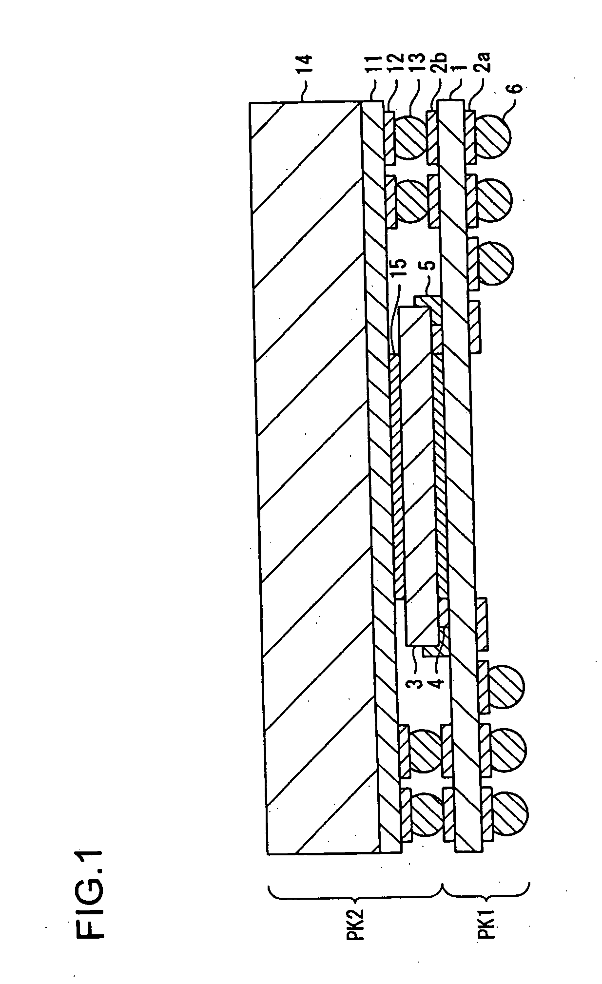
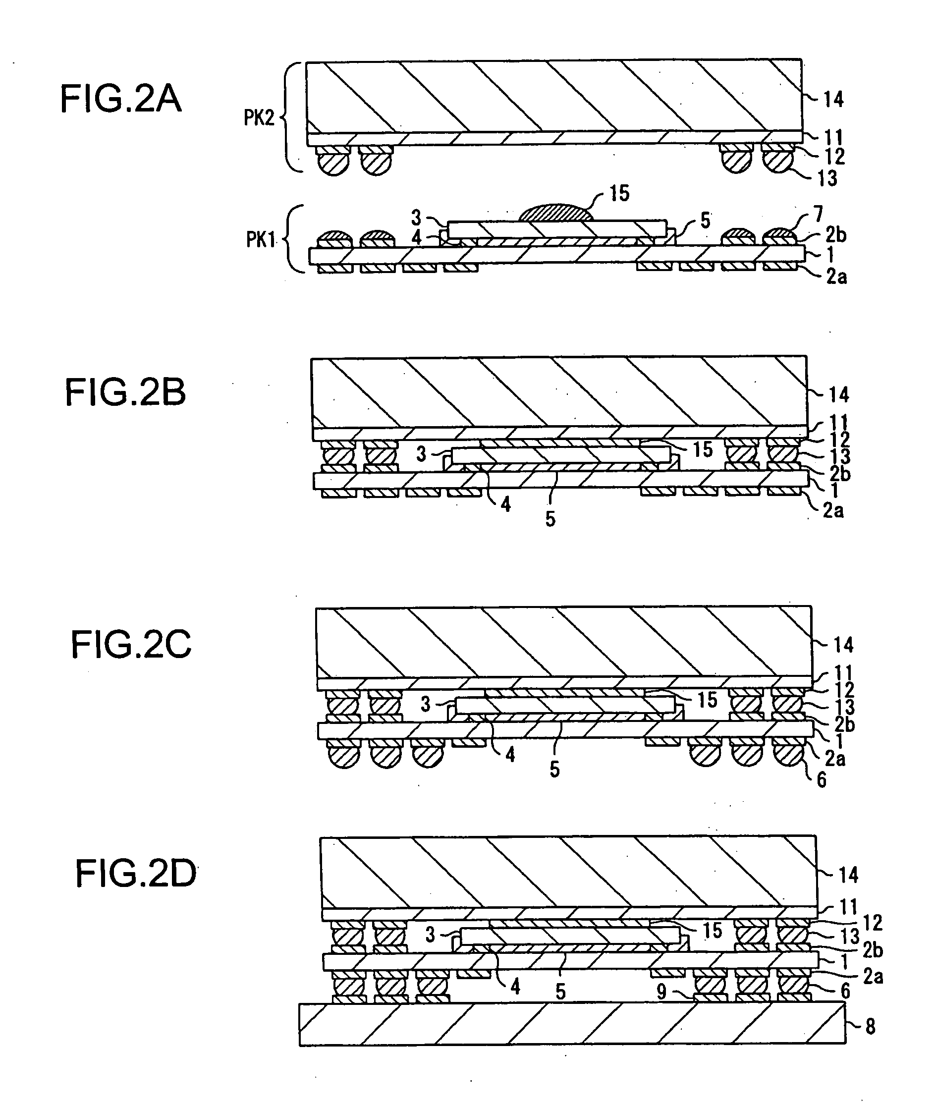
[0035]FIG. 1 is a sectional view schematically showing a structure of a semiconductor device according to the present invention.
[0036] Referring to FIG. 1, a semiconductor package PK1 includes a carrier substrate 1, and on both sides of the carrier substrate 1 are formed lands 2a and 2b, respectively. A semiconductor chip 3 is flip-chip mounted on the carrier substrate 1. Protruding electrodes 4 for flip-chip mounting are provided on the semiconductor chip 3. The protruding electrodes 4 provided on the semiconductor chip 3 are bonded to the lands 2b through an anisotropic conductive sheet 5 by Anisotropic Conductive Film (ACF) bonding.
[0037] Meanwhile, a semiconductor package PK2 includes a carrier substrate 11. Lands 12 are formed on a back surface of the carrier substrate 11, and protruding electrodes 13 are provided on the lands 12. A semiconductor chip is mounted on the carrier substrate 11. The carrier substrate 11, where the semiconductor chip is mounted, is sealed with a sea...
second embodiment
[0059]FIG. 3 is a sectional view schematically showing a structure of a semiconductor device according to the present invention.
[0060] Referring to FIG. 3, a semiconductor package PK11 includes a carrier substrate 21. Lands 22a and 22c are formed on both sides of the carrier substrate 21, respectively, and an internal wiring 22b is formed inside the carrier substrate 21. A semiconductor chip 23 is flip-chip mounted on the carrier substrate 21. Protruding electrodes 24 for flip-chip mounting are provided on the semiconductor chip 23. The protruding electrodes 24 provided on the semiconductor chip 23 are bonded to the lands 22c through an anisotropic conductive sheet 25 by ACF bonding. On the lands 22a provided on a back surface of the carrier substrate 21, provided are protruding electrodes 26 for mounting the carrier substrate 21 on a motherboard.
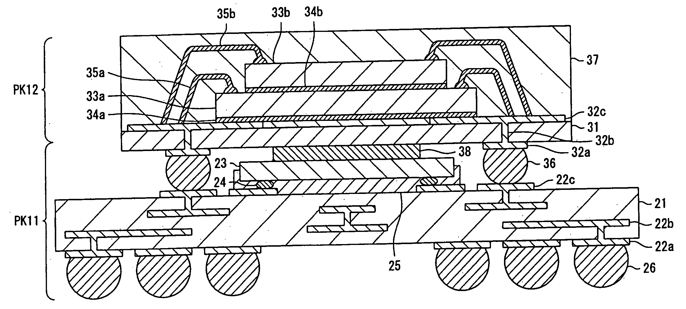
[0061] Meanwhile, a semiconductor package PK12 includes a carrier substrate 31. Lands 32a and 32c are formed on both sides of the carrier...
third embodiment
[0066]FIG. 4 is a sectional view schematically showing a structure of a semiconductor device according to the present invention.
[0067] Referring to FIG. 4, a semiconductor package PK21 includes a carrier substrate 41. Lands 42a and 42c are formed on both sides of the carrier substrate 41, respectively, and an internal wiring 42b is formed inside the carrier substrate 41. A semiconductor chip 43 is flip-chip mounted on the carrier substrate 41. Protruding electrodes 44 for flip-chip mounting are provided on the semiconductor chip 43. The protruding electrodes 44 provided on the semiconductor chip 43 are bonded to the lands 42c through an anisotropic conductive sheet 45 by ACF bonding. On the lands 42a provided on a back surface of the carrier substrate 41, provided are protruding electrodes 46 for mounting the carrier substrate 41 on a motherboard.
[0068] Meanwhile, a semiconductor package PK22 includes a carrier substrate 51. To the semiconductor chip 51, provided are electrode pads...
PUM
 Abstract
Description
Claims
Application Information