Semiconductor memory with virtual ground architecture

Inactive Publication Date: 2005-01-13
POLARIS INNOVATIONS
View PDF7 Cites 16 Cited by
  • Summary
  • Abstract
  • Description
  • Claims
  • Application Information

AI Technical Summary

Benefits of technology

[0008] A further preferred exemplary embodiment provides for the source / drain regions to be connected in pairs via connection regions which are arranged transversely with respect to the bit lines and simultaneously form so called “landing pads” for the contact-connection of the bit lines. In this exemplary embodiment, the bit lines may be arranged parallel at a distance from one another transversely with respect to the word lines in a conventional manner.

Problems solved by technology

However, the problem of a suitable arrangement of said bit lines for the top-side contact-connection of the source / drain regions arises in this case.

Method used


Image

  • Semiconductor memory with virtual ground architecture
  • Semiconductor memory with virtual ground architecture
  • Semiconductor memory with virtual ground architecture

Examples


Embodiment Construction

[0021] The making and using of the presently preferred embodiments are discussed in detail below. It should be appreciated, however, that the present invention provides many applicable inventive concepts that can be embodied in a wide variety of specific contexts. The specific embodiments discussed are merely illustrative of specific ways to make and use the invention, and do not limit the scope of the invention.

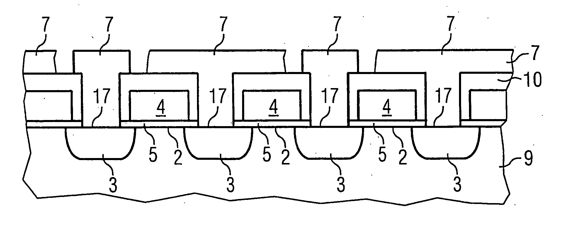
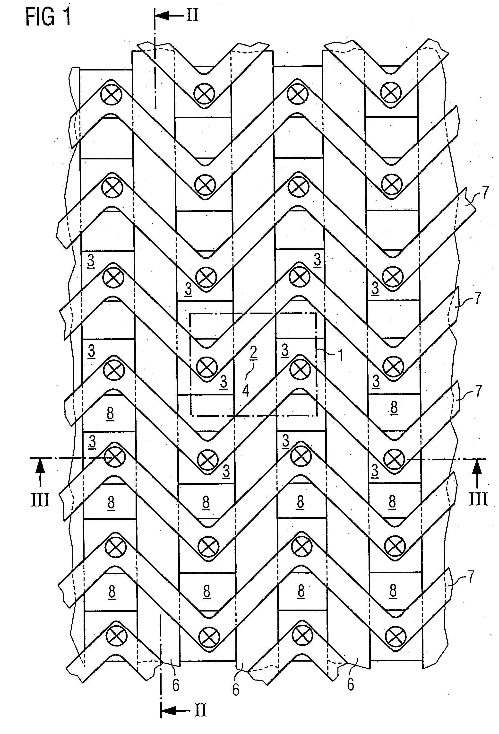
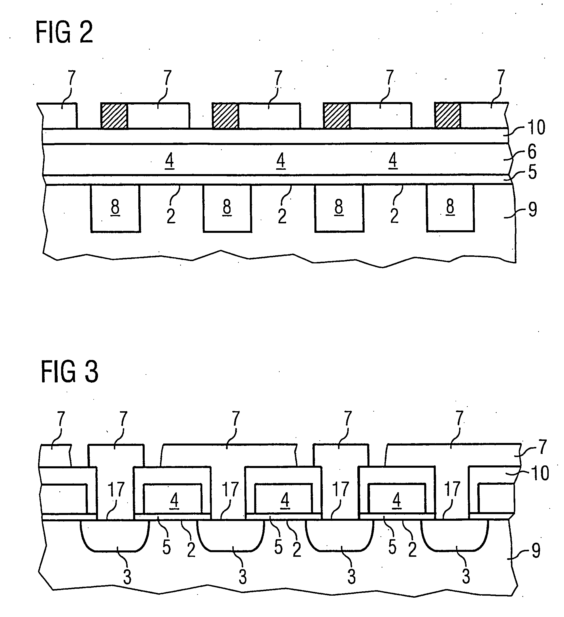
[0022]FIG. 1 illustrates a schematic plan view of an arrangement of the memory cells. A memory cell 1 is formed by a memory transistor that is emphasized by a border of broken lines. The associated memory transistor has a channel region 2, which is present in the semiconductor material below the word line 6, and source / drain regions 3. The gate electrode 4 above the channel region 2 is part of a word line 6. The gate electrode is isolated from the semiconductor material of the channel region by a thin gate dielectric, which, in the semiconductor memory described here, is fo...


PUM


Abstract

Insulation regions in the manner of STI isolations, which run transversely with respect to the word lines, isolate the source/drain regions of adjacent memory cells. Metallic bit lines are applied on the top side and patterned for example along zigzag lines such that the source/drain regions of a memory transistor which are contact-connected by the bit lines are in each case electrically connected by two mutually adjacent bit lines.

Description

TECHNICAL FIELD [0001] The present invention relates generally to a semiconductor memory device and more particularly to a semiconductor memory with virtual ground architecture. BACKGROUND [0002] A semiconductor memory comprises a row-wise and column-wise arrangement of memory cells each having a transistor structure. In the case of charge trapping memory cells, the gate dielectric is formed as a storage layer sequence made from three successive insulation layers, the central one of which is suitable for trapping charge carriers from the channel region, for example hot electrons in the channel (CHE, channel hot electrons) or electrons which pass from the channel into the storage layer by Fowler-Nordheim tunneling. This storage layer sequence may be for example a three-layered sequence of an oxide layer, a nitride layer and a further oxide layer, of which the oxide layers represent the boundary layers of the actual storage layer made of nitride. A charge trapping memory cell is erase...

Claims


Application Information

Patent Timeline
Patent Type & Authority Applications(United States)
IPC IPC(8): G11C16/04H01L21/8247H01L21/8246H01L27/115H01L29/788H01L29/792
CPCG11C16/0491H01L27/11568H01L27/115H10B43/30H10B69/00
Inventor RIEDEL, STEPHAN
Owner POLARIS INNOVATIONS
Why Eureka
Try Eureka